In this article, we analyze the static and dynamic behavior of some silicon carbide and gallium nitride FET devices. Companies are concentrating their efforts on these types of components that allow the creation of high-efficiency converters and inverters. This article is a follow-up to the previous one, which can be found here.
UnitedSiC’s UJ4SC075006K4S SiC FET MOSFET and Transphorm’s TP65H150G4PS GaN FET MOSFET for simulations
We’ll use some new-generation SiC and GaN FET devices in the tests and simulations that follow, which combine many of the benefits of newer technologies.
They can be summed up as follows:
- Excellent functioning at high temperatures
- Low input capacities
- Low RDS(on)
- Excellent reverse recoveries
- Presence of a diode for the elimination of extra voltages
- ESD protection
- Special packages for fast switching and cleaner waves
The devices under examination, shown in Figure 1, are:
- UnitedSiC’s UJ4SC075006K4S SiC FET MOSFET
- Transphorm’s TP65H150G4PS GaN FET MOSFET

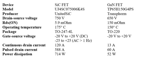
The first UJ4SC075006K4S device is very powerful, with an on-resistance (RDS(on)) of only 6 mΩ and 750 V, and is part of UnitedSiC’s nine-piece family of SiC FET MOSFETs. The component is based on the unique configuration of the “cascode” circuit. With an RDS(on) less than half that of the competition, the device features a short-circuit withstand time of 5 µs. The samples are available in TO-247-4L packages, with four pins, and some in TO-247-3L packages, with three pins. The cascode technique offers the advantages of wide-band–range technology, such as high speed, low losses with high temperature operation, great stability, and robustness with integrated ESD protection. For switching applications, the integrated diode is much faster than competing technologies. Its applications include drives and traction for electric vehicles, on-board and off-board chargers, one-way and two-way power converters, inverters for renewable energy, and converters for all types. The second TP65H150G4PS device is a 650-V, 150-mΩ GaN specimen and is a normally off component. It combines the high-voltage GaN HEMT technology with the low-voltage technology of the silicon MOSFET, offering highly reliable operation and excellent performance. The most important characteristics of the two power devices can be seen in the table below.
Efficiency and RDS(on) in the static regime
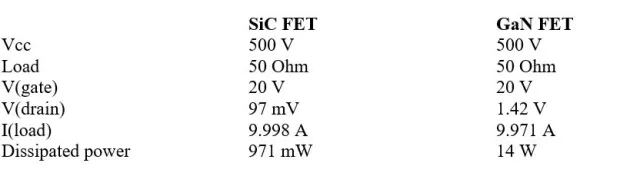
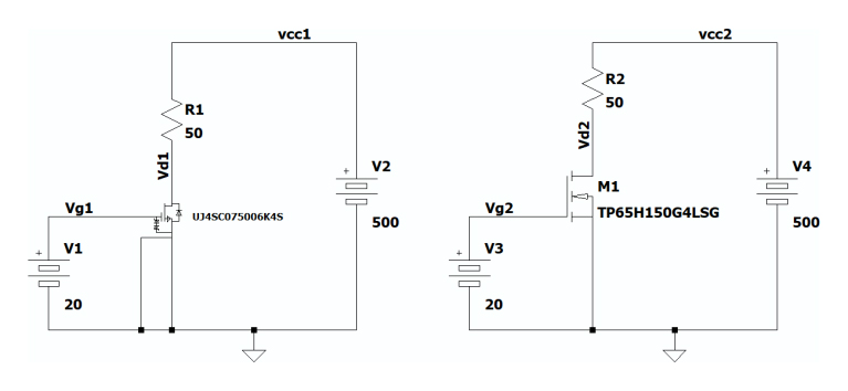
The following simulation is used to evaluate and check the efficiency values of a power supply circuit in the static regime, with the verification of the resistance of the drain-source channel when the device is switched on. The diagram in Figure 2 shows the two devices under examination in the on state, the latter secured with a direct voltage of 20 V on the gate. The system power supply is 500 V for a 50-Ω load. The following table shows the measured data:
The calculation of the RDS(on) of both components is carried out during the on state of the devices by carrying out the following equations:

The efficiency calculation is also very simple and is used to evaluate the amount of energy used profitably in the system and, by difference, that lost in unused heat:

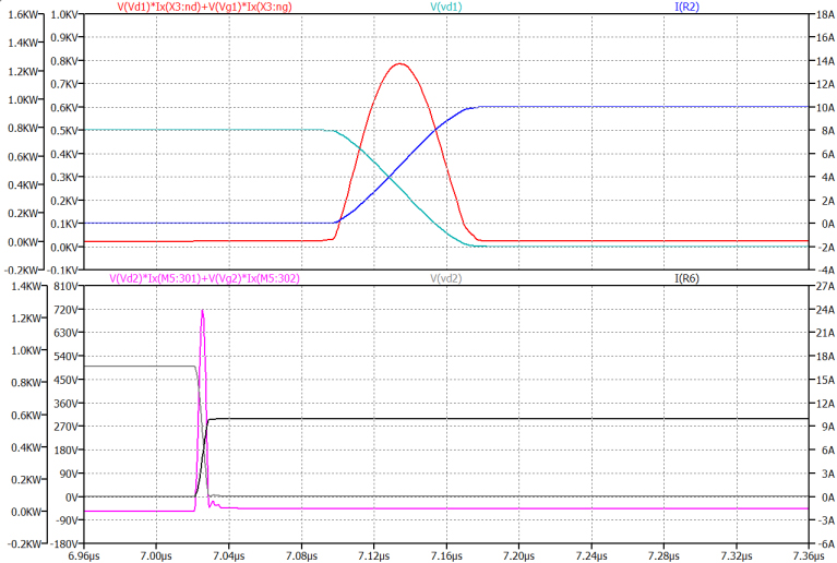
Efficiency and power losses in the dynamic regime
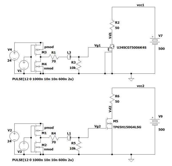
The dynamic regime is the most important, as it is here that the components are put to the test. The systems are subject to a lot of stress due to EMI, power losses, any inductive loads connected, and the switching of the components themselves. Figure 3 shows a generic example of a PWM power supply whose frequency is, in this case, about 500 kHz. The generation of the PWM signal takes place through two monolithic P- and N-channel MOSFETs. The reduction of some types of noise is carried out through a ferrite bead characterized by the following features:
- Inductance: 0.38 µH
- Series resistance: 0.371 Ω
- Parallel resistance: 1,600 Ω
- Parallel capacitance: 0.78 pF
- Impedance to 100 Mhz: 266.5 Ω
- Max. impedance: 1,598.1 Ω
- Frequency of max. impedance: 292 MHz
Technology is fighting the battle against power outages (Figure 4). The components’ non-ideal nature increases their dissipated power precisely at switching moments.
The presence of the component’s input and output capacity, as well as its RDS(on) and other elements, contributes to power losses, which are fortunately improving day by day.
The following is the efficiency achieved by the operation of the two devices:
- SiC FET efficiency: 98.24%
- GaN FET efficiency: 99.02%
These are extremely high efficiencies, allowing almost all of the energy to be used actively while keeping the MOSFETs’ operating temperatures low.
In fact, the Vds value in the on state is very low, and the electronic switches behave almost perfectly.
The simulation can be carried out only if the relative SPICE libraries of the two components used are available, are downloadable from the internet, and include the following header:
.subckt UJ4SC075006K4S nd ng ns nss
and
.subckt TP65H150G4LSG 301 302 303
Conclusion
Designers should keep in mind that electronic simulations with power devices may differ significantly from reality, especially if the systems contain inductive and capacitive components.
Furthermore, it should be remembered that power MOSFETs always need to be driven by excellent drivers, which ensure a high driving current at the gate, as the capacitive input components hinder the clear and immediate activation right at the gate.