For decades, silicon has dominated the transistor world, but that has been gradually changing. Compound semiconductors made of two or three materials have been developed and offer unique benefits and superior characteristics. For example, compound semiconductors gave us the LED: One type is made up of a mix of gallium arsenide (GaAs) and gallium arsenide and phosphorus (GaAsP); others use indium and phosphorus.
While compound semiconductors are harder to make and more expensive, they offer significant benefits over silicon. Designers of new, more demanding applications such as automotive electrical systems and electric vehicles (EVs) are finding that compound semiconductors better meet their stringent specifications.
Two compound semiconductor devices that have emerged as solutions are gallium nitride and silicon carbide power transistors. These devices compete with the long-lived silicon power LDMOS MOSFETs and superjunction MOSFETs. GaN and SiC devices are similar in some ways but have significant differences. This article compares the two and offers information to help you make a decision for your next design.
Wide-bandgap semiconductors
Compound semiconductors are referred to as wide-bandgap devices. Without resorting to a review of crystal lattice structures, energy levels, and other mind-numbing semiconductor physics, let’s just say that the definition of WBG attempts to describe how current (electrons) flows in a compound semiconductor.
WBG compound semiconductors have high electron mobility and higher bandgap energy, translating into characteristics that are superior to silicon’s. Transistors made from WBG compound semiconductors have higher breakdown voltages and greater tolerance for high temperatures. These devices are superior to silicon equivalents for high-voltage and high-power applications.
WBG transistors also switch faster and can operate at higher frequencies than silicon. Lower on-resistance means they dissipate less power, thereby promoting efficiency. This unique combination of characteristics makes these devices attractive for some of the most demanding circuits used in automotive applications, especially hybrid electric vehicles (HEVs) and EVs.
GaN and SiC transistors are becoming readily available to address the challenges of automotive electrical equipment. The key takeaways for GaN and SiC devices are these advantages:
- High-voltage capability with devices for 650, 900, and 1,200 V
- Faster switching speed
- Higher operating temperature
- Lower conduction resistance with minimum power dissipation and greater efficiency
GaN transistors
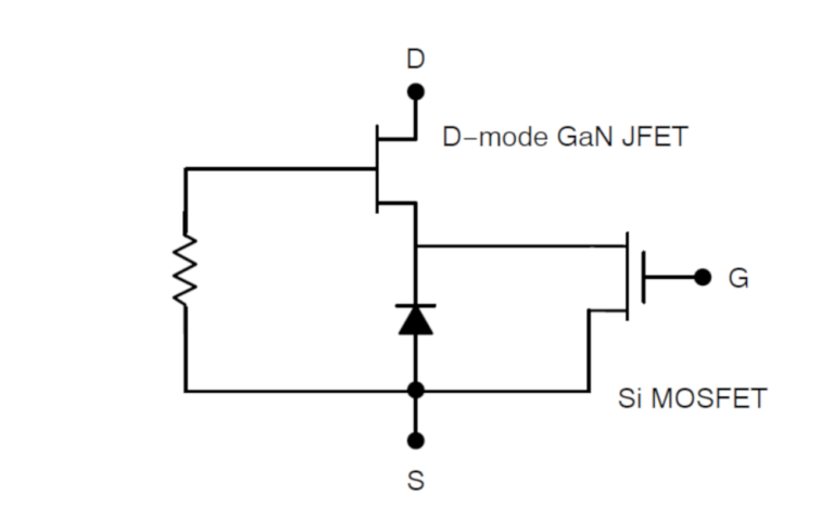
GaN transistors found an early niche in the radio-frequency (RF) power field. The nature of the materials led to the development of a depletion-mode (d-mode) field-effect transistor (FET). Known as a pseudomorphic high-electron–mobility transistor (pHEMT), d-mode FETs are naturally “on” devices; with no gate control input, a natural conduction channel exists. Gate input signals control the channel conduction and turn the device on and off.
Because normally “off” enhancement-mode (e-mode) devices are preferred in switching applications, this led to the development of e-mode GaN devices. The first was a cascode of two FET devices (Figure 2); now, standard e-mode GaN devices are available. They can switch at frequencies up to 10 MHz and up to tens of kilowatts.
GaN devices are widely used in wireless equipment as power amplifiers at frequencies up to 100 GHz. Some of the primary use cases are cellular base station power amplifiers, military radar, satellite transmitters, and general RF amplification. However, because of their high voltage (up to 1,000 V), high temperature, and fast switching, they have also been incorporated into a variety of switch-mode power supply applications such as DC/DC converters, inverters, and battery chargers.
SiC transistors
SiC transistors are natural e-mode MOSFETs. These devices can switch at frequencies as high as 1 MHz at voltage and current levels much higher than silicon MOSFETs. Maximum drain-source voltage is up to about 1,800 V with a current capability to 100 A. In addition, the on-resistance of SiC devices is much lower than that of silicon MOSFETs, making them more efficient in all switching power applications. One key disadvantage is that they require a higher gate drive voltage than other MOSFETs, although this is changing as designs improve.
SiC devices need 18 to 20 V of gate drive voltage to turn on the device with a low on-resistance. Standard Si MOSFETs require a gate of less than 10 V for full conduction. In addition, SiC devices need a –3- to –5-V gate drive for switching to the “off” state. However, special gate drive ICs have been developed to meet this need. SiC MOSFETs are generally more costly than other alternatives, but their high-voltage, high-current capabilities make them well-suited to automotive power circuits.
WBG transistor competition
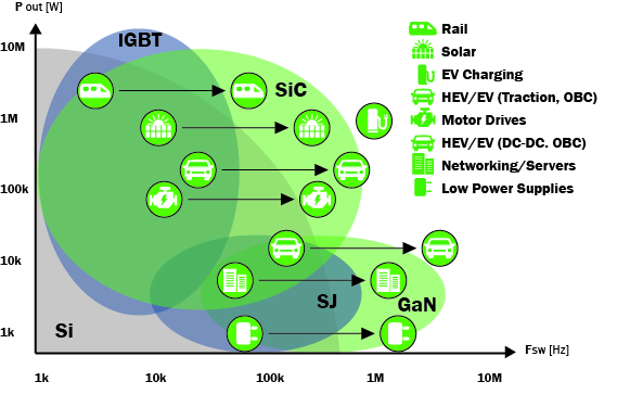
Both GaN and SiC devices compete with other well-established semiconductors, specifically Si LDMOS MOSFETs, superjunction MOSFETs, and IGBTs. In many applications, these older devices are gradually being replaced by GaN and SiC transistors.
For example, IGBTs are being replaced by SiC devices in many applications. SiC devices can switch at higher frequencies (100 kHz or higher, versus 20 kHz), thereby reducing the size and cost of any inductors or transformers while increasing efficiency. SiC can also handle more current than GaN.
Summarizing the GaN versus SiC comparison, here are the highlights:
- GaN switches faster than Si.
- SiC operates at higher voltages than GaN.
- SiC requires high gate drive voltage.
- Superjunction MOSFETs are gradually being replaced by both GaN and SiC. SiC appears to be the favorite for on-board chargers (OBCs). This trend will undoubtedly continue as engineers discover the newer devices and gain experience with them.
Automotive applications
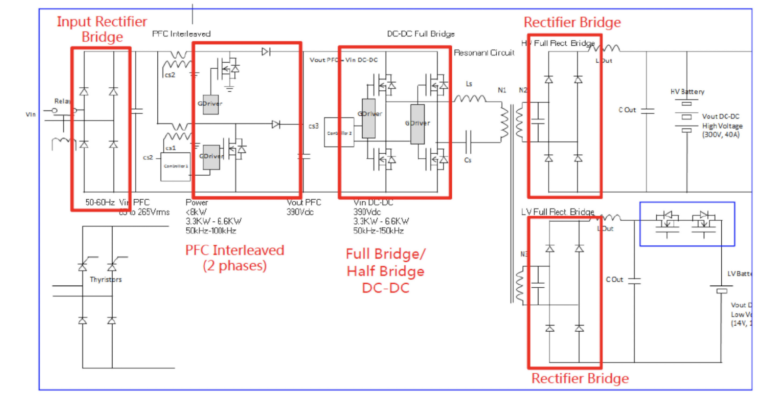
Many power circuits and devices can be improved by designing with GaN and SiC. One of the biggest beneficiaries is automotive electrical systems. Modern HEVs and EVs contain equipment that can use these devices. Some popular applications are DC/DC converters, OBCs, motor drivers, and LiDAR. Figure 3 points out the main subsystems in an EV that require high-power switching transistors.
DC/DC converters
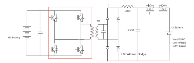
These power circuits convert the high battery voltage down to a lower voltage to operate other electrical equipment. Battery voltages now range up to 600 or 900 V. A DC/DC converter drops this down to 48 or 12 V or both for the operation of other electronic components (Figure 3). In HEVs and EVs, a DC/DC converter can also be used on the high-voltage bus between the battery pack and the inverter.
OBCs
Plug-in HEVs and EVs contain an internal battery charger that connects to an AC power source. This allows at-home charging without an external AC-to-DC charger (Figure 4).
Traction motor driver
The traction motor is the high-output AC motor that drives the vehicle’s wheels. The driver is an inverter that converts the battery voltage into three-phase AC that operates the motor.
LiDAR
LiDAR refers to a technology that incorporates both light and radar methods to detect and identify surrounding objects. It scans an area of 360˚ with a pulsating infrared laser and detects the reflected light. This information is translated into a detailed 3D picture of the scenes out to about 300 meters, with a resolution of several centimeters. Its high resolution makes it an ideal sensor for vehicles, especially self-driving, to improve the identification of nearby objects. LiDAR units operate from a DC voltage in the 12- to 24-V range that is derived from a DC/DC converter.
Because of their high voltage, high current, and rapid switching, both GaN and SiC transistors offer the automotive electrical designer forgiving and easier designs as well as superior performance.