FPGA or Field-Programmable Gate Array can be defined as integrated circuits semiconductors that are designed to be flexible and programmable by users to fit defined or specialized functions. Thus, unlike traditional application-specific integrated circuits, ICs, (ASICs), designed to perform specific tasks, FPGA can be reprogrammed. They are thus commonly known as field programmable.
The ability to be reprogrammed and reconfigured an unlimited number of times is what gives the FPGA an edge over other IC. With it, users can define and redefine sets of instructions to implement their digital circuits by specifying logic functions and interconnection. This makes FPGA suitable for most projects, from prototyping, development, manufacturing, digital processing, networking and so much more. In this article, we will explore what are FPGA and where they are used.
Let’s have a look.
To understand FPGA, it is important to first understand what are ICs, Integrated Circuits, as they are the basis of CPUs, GPUs and FPGA. They are used to implement digital logic, using very small electronic circuits. Usually, these miniature electronic circuits contain several millions or hundreds of millions of electronic components such as capacitors, and transistors, all built onto a single piece of semiconductor material. To learn more about ICs you can see this article here How Is a Microprocessor Different from an Integrated Circuit?
The FPGA development and implementation have more than ever blurred the lines between hardware and software engineering. These devices give engineers a leeway to interact with hardware and manipulate the physical attributes of logic, and interconnections through programming, typically using hardware description languages (HDLs). These languages effectively bridge the gap between hardware and software programming.
Due to their versatility and programmability, FPGAs are able to provide different functionality and benefits to different electronic circuits and appliances. Numerous sectors and markets, medical, and aerospace sectors from aircraft navigation systems to medical scanners: including wireless communications, data centres, and the automotive, use FPGAs.
What is FPGA?
Based on the acronym FPGA stands for Field Programmable Gate Arrays. These are integrated circuits, ICs that are designed with grids of configurable logic blocks (CLBs) and programmable interconnects. With these ICs, the functionality, interconnects and logic of the device can be changed; either during manufacturing or by programming the device during use. FPGAs as integrated circuits fall under programmable logic devices.

Figure 1: Xilinx FPGA
The ability to be programmed and reprogrammed is a feature that sets FPGAs from the older Application Specific Integrated Circuits (ASICs). ASICs unlike FPGA are made with an explicit specific goal and function in mind since development and cannot be altered or reconfigured post-manufacture. Making them useful in One Time Programmable (OTP) devices. FPGA also offer a variation that can perform the OTP option. However, the most popular types are based on static random-access memory (SRAM), which allows for reprogramming as the design evolves.
FPGAs were introduced in programmable logic devices in the early 80s, with the first commercial use being in 1985 by AMD. Until the 90s however, only a few contenders were known in the FPGA market including Xilinx, TI, Altera and Intel. To date, AMD is one of the dominating members in the market with a 60-70% stake in the market.

Figure 2: Xilinx FPGA development Spartan6 board
How an FPGA Works
Understanding how FPGAs work is straightforward. The use of FPGA involves only programming the configurable logic blocks and interconnects using many of the many different programming languages. The process involves understanding the requirements of the circuit and how to program the FPGA. The storage is RAM-based memory and thus can be reconfigured an unlimited number of times.
A matrix of programmable interconnects and customizable logic blocks (CLBs) make up FPGAs (Field-Programmable Gate Arrays). These are the fundamental building blocks, CLBs, can be customised to carry out a variety of digital logic operations. CLBs comprise programmable routing controllers
(multiplexers), two 16-bit function generators, one 8-bit function generator, two registers (flip-flops or latches), and two registers. Macros and other designed functions are implemented using CLBs.
To better understand how FPGAs work it is important to understand what is inside, its architecture. Let’s have a look:
The architecture of an FPGA
The architecture of each FPGA vendor is specified differently. The components of each FPGA are specialised and designed with specific functions and capacities. The following are some of the essential elements, guiding principles, and capabilities:

Figure 3: Example of an FPGA
- Configurable Logic Block
Configurable Logic Blocks (CLBs) serve as the core building blocks at its heart. CLBs are made up of look-up tables (LUTs) and flip-flops. The LUTs can be programmed to perform a variety of digital logic functions, whilst the flip-flops support sequential logic operations, allowing data to be stored and state machines to be formed.
FPGAs use a matrix of programmable interconnects to enable communication and data flow between CLBs. These interconnections constitute a web of connections that may be dynamically modified, making it possible to create bespoke data channels. This capability enables FPGA designers to adapt the chip's architecture to specific applications while optimising performance.
- Flip-Flops
Flip-Flops are basic sequential logic elements that reside within an FPGA's CLBs. Their major duty is to store binary data and serve as the foundation for the FPGA's sequential operations and memory. When activated by a clock signal, these flip-flops alter (toggle) their state, allowing synchronous logic architecture. Counters, shift registers, and finite state machines are examples of applications that require memory elements or sequential decision-making.
- Lookup Tables
Look-Up Tables (LUTs) are components within Configurable Logic Blocks (CLBs). LUTs are tiny blocks of memory that include truth tables that map all conceivable input combinations to their matching output values for certain logic functions. FPGA designers can construct any desired Boolean function within the FPGA by programming the values contained in these LUTs. This capability provides extraordinary versatility, allowing designers to easily develop unique logic circuits, making FPGAs so versatile and adaptable to a wide range of jobs.
- DSP Slices
Digital Signal Processing (DSP) slices or blocks are specialised hardware pieces designed to execute digital signal processing operations efficiently. They include specialised multipliers, accumulators, and other components for performing rapid and parallel arithmetic operations. These DSP blocks shine in filtering, image and audio processing, telecommunications, and other signal-processing applications where the ability to do complicated mathematical computations quickly is critical.
Memory blocks are another important component of FPGAs, as they provide on-chip storage for data and instructions. FPGAs frequently include memory blocks such as Random-Access Memory (RAM) and Read-Only Memory (ROM). RAM blocks are ideal for temporary data storage or buffer solutions since they provide both read and write operations. ROM blocks, on the other hand, are utilised to store unchanging data or constants required during FPGA operation. Memory blocks are essential in applications requiring fast and efficient data access, such as digital signal processing, picture processing, and data buffering.
- Transceivers
Transceivers are designed to send and receive serial data at fast rates to and from the FPGA. This specialised component enables the deployment of high-speed data transport without depleting the FPGA's logic resources.
- Input/Output Blocks
The FPGA's Input/Output Blocks (IOBs) act as a bridge between the outside world and the semiconductor. They are in charge of interacting with external devices, as well as adapting different voltage levels, I/O standards, and protocols. This versatility enables the FPGA to integrate with a variety of systems and interfaces.
How to use an FPGA and its Applications
FPGAs have a wide array of applications in modern technologies, ranging from everyday use to industrial setups. The reliance on FPGA can be attributed to their versatility, accelerated function and performance that would otherwise be very daunting tasks in software. Some of these tasks include deep learning neural networks, artificial intelligence, computing algorithms and other IoT applications.
The FPGA is initially unprogrammed and must be programmed to define its functionality. During the configuration phase, the appropriate logic functions and interconnections are specified using a
hardware description language (HDL) such as VHDL or Verilog. The HDL code explains the digital circuit's behaviour and structure. This is unlike programming GPUs or CPUs, in this case, you are writing code that changes the hardware to a desired outcome.
The HDL code is synthesised into a netlist, which represents the logical connections and circuit components. The code is turned into a binary file that can be loaded up into the FPGA. The HDL code is analysed, optimised, and changed during synthesis into a format suitable for FPGA implementation.
The synthesised netlist is assigned to specified FPGA resources. The placement method dictates which logic functions should be implemented in which FPGA CLBs. The HDL physically changes the hardware. It also considers aspects such as timing limitations, signal routing, and available resources.
How to Program FPGAs
Using the word programming can be loosely interpreted when dealing with FPGAs, due to how they work. It is not exactly creating software or code that runs on a software level but rather creating a program that works on a hardware level, and designing a circuit. Hence the name Hardware Description Languages (HDLs).

Figure 4: Programming an FPGA
Several mainstream HDLs are used to program FPGAs. Here are a few common ones:
VDHL: VHDL is an abbreviation for VHSIC (Very High-Speed Integrated Circuits) Hardware Description Language, which initially debuted in the 1980s and was based on Ada and Pascal.
Verilog - The first HDL ever designed, Verilog is mostly used for test analysis and verification nowadays. This language's core was built on C.
Lucid - This language was designed exclusively for FPGAs and avoids some of the drawbacks of older languages like Verilog.

Figure 5: Comparing Verilog to VDHL
Most HDLs are low-level languages and are harder to deal with compared to modern programming languages making them only familiar to hardware engineers. Although some are very advanced and similar to modern software languages most software developers are still too unfamiliar. However, with the help of unified platforms and other tools, software developers can write code in the preferred high-level languages to program FPGAs.
These platforms function by effectively translating higher-level languages to lower-level languages, allowing an FPGA to do the needed function. Some languages that can be used to programme FPGAs with unified software platforms include:
TensorFlow and Pytorch AI frameworks - With Vitis AI, AI scientists can now easily build their taught deep learning models from TensorFlow or Pytorch for FPGA acceleration. This not only eliminates the requirement for low-level hardware programming but also provides a blazing-fast compilation time in minutes, comparable to the typical software compiling experience using CPUs and GPUs.
Python – Python is perhaps the most vastly used programming language by engineers, software developers and programmers. With its vast libraries and ease of programming, designers may use the Python language and libraries to construct high-performance programmes FPGAs with PYNQ, an open-source initiative from AMD that simplifies the use of AMD platforms.
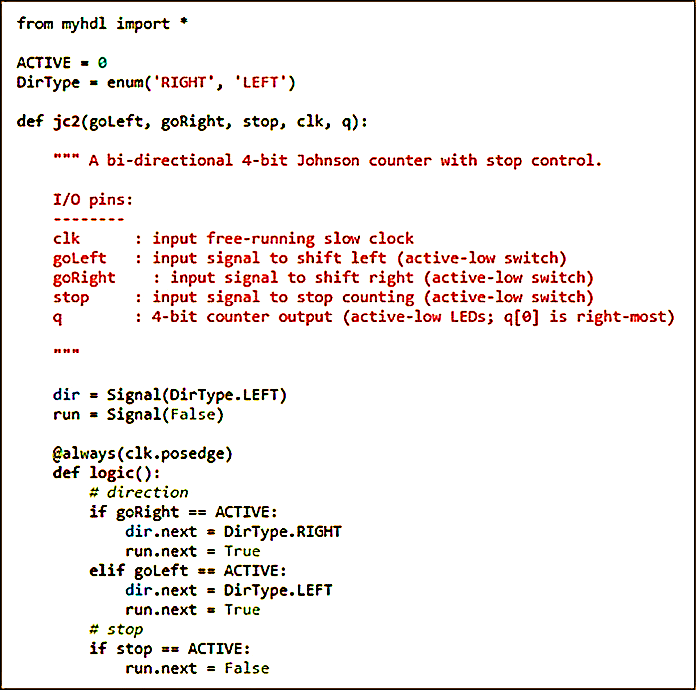
Figure 6: HDL in Python Using MyHDL
C and C - C-based languages can now be used to create FPGAs thanks to high-level synthesis (HLS). The AMD Vivado HLS compiler, in particular, provides a programming environment for the optimisation of C and C programmes that shares important technology with both conventional and specialised processors. This enables software programmers to optimise code without being constrained by restricted memory space or processing resources.

Figure 7: Using Vivado
Applications of FPGA
FPGAs are employed in a wide range of applications:
- Digital signal processing,
- biomedical instrumentation,
- device controllers,
- software-defined radio,
- medical imaging,
- computer hardware emulation,
- speech recognition,
- cryptography,
- filtering and communication encoding,
Some other specialized applications that use FPGAs might include their use in:
- Smartphones,
- self-driving cars, cameras,
- displays; video and image processing,
- and security systems are examples of consumer electronics applications.
Final Thoughts
Finally, future FPGA architecture developments are likely to revolve around even better integration of specialised hardware blocks, enhanced DSP capabilities, and larger memory capacity. The emphasis will be on catering to upcoming technologies like artificial intelligence, edge computing, and 5G, pushing FPGAs to deliver improved performance, energy efficiency, and adaptability for tomorrow's issues.