High dv/dt transients are the reason behind challenges when designing the electronic converters that use the wide band gap (WBG) devices that are usually cause in the form of the parasitic parameters that are present in active and passive components of them [1][2][3][4]. It has been noted that the dv/dt of the WBG devices is bigger than the Si-based IGBTs that are known to be widely used for high-power converters design. Comparison between the Si based modules and SiC-MOSFET-based modules based on their switching speed can be observed in Table 1. Two parasitic capacitances that are dominant in nature, the parasitic turn-to-turn and turn-to-core capacitance have been identified specifically for the filter inductors [5][6]. Two of the modeling methods have been detailed out for the analysis purpose of the parasitic capacitances. It can be noted here that the two capacitances that are known as turn-to-turn and turn-to-core have been combined to make an equivalent capacitance [7]. Capacitance of the inductors is different, it completely depends upon the voltage potential of the core and voltage of the winding fix or attach this core [8]. When the core is in floating state, the voltage potential of the magnetic core of inductors and transformers will be higher compared to medium voltage applications. A network having three terminals is formed by the transformer and the inductors with a ground connection. Switching behaviors of the devices MV SiC MOSFET and the effects that the core/frame-floating and the core/frame grounded inductors have on them have been compared in this article. Finally, the accuracy of the SiC MOSFET double pulse test is validated by experimental test that is based on 10kV of the SiC MOSFET double pulse test.
For more information about this article, please visit its original version.
 Table 1: Switching speed comparison
Comparison of Frame-Floating and Frame- Grounded MV Inductors
Figure 1 shows the analyzed MV 30mH inductor. It has been rated at the level of 10 A and is based on the nanocrystalline magnetic core. Double pulse test in the laboratory circuit diagram is shown in Figure 2. Power module of the custom packaged half-bridge 10 kV SiC MOSFET enables the double pulse setup [2]. High frequency currents are measured precisely by the help of the 200 MHz PearsonTM 2877 monitors [10]. Two cases have been used to test this similar pulse test. In case 1, no ground connection is made on the MV inductor that is tested or it can be said that the core/frame is floated whereas, in case 2 the core/frame has been grounded which means that one ground connection has been provided from the ground point of MV inductor to the ground of the dc-link busbar [12]. Figure 3 shows the results of the experiment for the test conducted at 3 kV link voltage having the 12 A peak load current. Figure 4 shows the impact that the ground current has on the whole power circuit along with the clear mentioning of the paths of the load and ground current. With the help of this experiment it can be concluded that the ground current is added only to the id (HS MOSFET current) at the time of the turn-off period and in opposition to this concept the ground current is added to id- (LS MOSFET current) at the time of the turn-on period. High frequency components increase the electromagnetic inference due to which the energy dissipation increases during switching.
 Figure 1: MV inductor 30mH
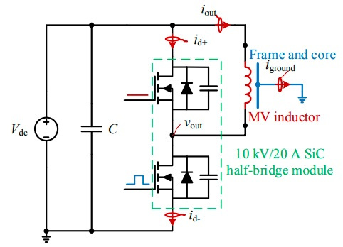 Figure 2: Circuit diagram of Double pulse test setup
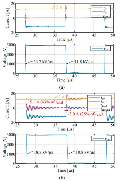 Figure 3: Experimental results with (a) floated core/frame (b) grounded core/frame
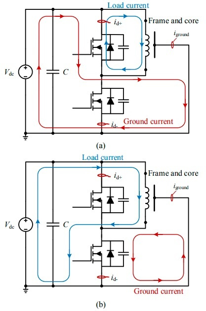
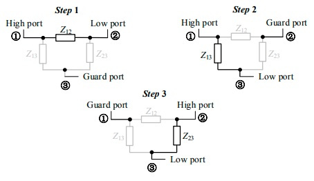
General Three-Terminal Equivalent Circuit
This portion of the article is all about the introduction of the general three-terminal equivalent circuit that has been formulated for the capacitive couplings existing between winding-to-winding and winding-to-ground [11]. Figure 5 (a) shows the schematic of the inductor with core/frame grounded whereas Figure 5 (b) shows the impedance addressing the capacitive coupling between arbitrary two terminals. Here, the terminal 1 and 2 represent the power connection and the terminal 3 represents the connection of the frame/core ground. Figure 6 clearly shows the three steps performed with guarding technology for the measurement of the impedances.
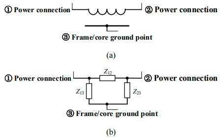 Figure 5: Equivalent circuit for inductor
Simulations and Experimental Validations
To simplify the simulations mentioned, it is important to identify the Y13 of the MV inductor. A Figure 7 shows a comparison between the fitted admittance and the measured admittance. Simulations have shown that the measured output voltage with the MV double pulse test matches the excitation voltage. With higher dv/dt the ground current increases in a non-linear way as the impedance between the terminals is not a first order system [12].
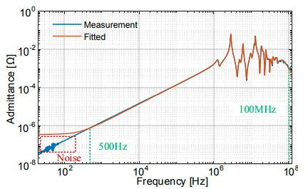 Figure 7: Comparison between fitted and the measured admittance
Conclusion
This article has analyzed the ground current in the filter inductors of the MV SiC-MOSFET based converters in the case when core/frame is grounded. This is actually considered as a common solution for high power inductors. The behavioural model shown in this article has the ability of simulating the ground current of an inductor double pulse test. Under the higher potential of the voltage dv/dt the ground current increases in a non-linear manner that is helpful in the process of balancing the design of the power modules, gate drivers and filters.
References
[1] F. Wang, Z. Zhang, and E. Jones, “Wide bandgap device characterization”, in Professional Education Seminar of 2016 Applied Power Electronics Conference, Mar. 2016, pp.1-139.
[2] A. B. Jørgensen, N. Christensen, D. N. Dalal, S. D. Sønderskov, S. Bęczkowski, C. Uhrenfeldt, and S. Munk-Nielsen, “Reduction of parasitic capacitance in 10kv SiC MOSFET power modules using 3d fem,” in Proc. 2017 19th European Conference on Power Electronics and Applications (EPE’17 ECCE Europe), Nov. 2017, pp. 1-8.
[3] N. Christensen, A. B. Jørgensen, D. N. Dalal, S. D. Sonderskov, S. Bęczkowski, C. Uhrenfeldt, and S. Munk-Nielsen, “Common-mode current mitigation for medium voltage half-bridge SiC modules,” in Proc. 2017 19th European Conference on Power Electronics and Applications (EPE’17 ECCE Europe), Nov. 2017, pp. 1-8.
[4] D. N. Dalal, N. Christensen, A. B. Jørgensen, S. D. Sønderskov, S. Bęczkowski, C. Uhrenfeldt, and S. Munk-Nielsen, “Gate driver with high common-mode rejection and self-turn-on mitigation for a 10 kv SiC MOSFET enabled MV converter,” in Proc. 2017 19th European Conference on Power Electronics and Applications (EPE’17 ECCE Europe), Nov. 2017, pp. 1-8.
[5] A. Massarini and M. K. Kazimierczuk, “Self-capacitance of inductors,” IEEE Transactions on Power Electronics, vol. 12, no. 4, pp. 671–676, Jul. 1997.
[6] A. Ayachit and K. Kazimierczuk, “Self-capacitance of single-layer inductors with separation between conductor turns,” IEEE Transaction on Electromagnetic Compatibility, vol. 59, no. 5, pp. 1642–1645, Sep. 2017.
[7] E. Snelling, SoftFerrites: Properties and Applications. London, U.K.: Iliffe Books Ltd., 1988.
[8] Z. Shen, H. Wang, Y. Shen, Z. Qin and F. Blaabjerg, “An Improved Stray Capacitance Model for Inductors,” IEEE Transactions on Power Electronics, vol. 34, no. 11, pp. 11153-11170, Nov. 2019.
[9] IEEE Standard for General Requirements for Dry-Type Distribution and Power Transformers, IEEE Standard C57.12.01-2015, 2015.
[10] “Pearson Electronics”. [Online]. Available: https://www.pearsonelectronics.com/, [Accessed Nov. 20, 2019].
[11] Lennart Ljung, “System Identification Toolbox User’s Guide” [Online], Available: https://se.mathworks.com/help/pdf_doc/ident/ident.pdf, [Accessed Nov. 20, 2019].
[12] Behavioral Modeling of Ground Current in Filter Inductors of Medium-Voltage SiC-MOSFET-Based Converters. Hongbo Zhao, Dipen Narendra Dalal, Jannick Kjær Jørgensen, Xiongfei Wang, Michael Møller Bech, Asger Bjørn Jørgensen, Szymon Beczkowski, Christian Uhrenfeldt and Stig Munk-Nielsen Department of Energy Technology, Aalborg University, Aalborg, Denmark