This article presents three different designs affecting measurements of a non-invasive contactless current sensor. The converter is a two-phase DC/DC GaN converter with 120VDC input operating at 6.7MHz. 120VDC is a standard voltage level in the secondary power system at the International Space Station (ISS).
Gallium nitride (GaN) devices enable high-frequency, high-density power supplies desirable in aerospace, transportation, and medical applications. Certain design rules must be considered in laying out the printed-circuit board (PCB) and components. For instance, a multi-layer layout and tracing with copper pores would reduce the conduction path length and minimize the parasitic elements consequently. Inserting a current sensor into the PCB is always a challenge. Most current sensors require split traces going in and out of the sensor module. Certain board areas should also be added to dissipate the heat caused by the current passing into the sensor with split traces. Contactless current sensors minimize the trace lengths and require no additional thermal considerations other than the converter operating temperature. However, certain design rules are still required to achieve accurate measurements. This article presents three designs affecting measurements of a non-invasive contactless current sensor developed by Tell-i Technologies. The converter is a two-phase DC/DC GaN converter with 120-VDC input operating at 6.7 MHz. 120 VDC is a standard voltage level in the secondary power system at the International Space Station (ISS).
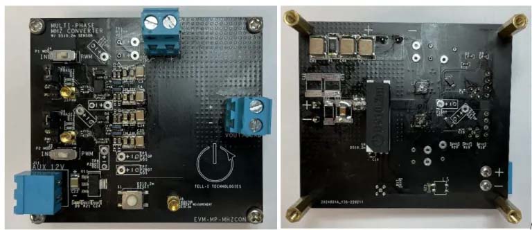
Multi-phase megahertz converter SDK
Using GaN MOSFET’s high power density and ultra-fast switching, Tell-i’s newly developed SDK board uses two phases to exceed normal switching speeds. Supporting a standard 120-V bus voltage, as used in systems like the ISS, the multi-phase configuration allows interleaving converters to achieve effective switching at 3 MHz, 5 MHz, and an outstanding 6.87 MHz.
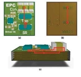
At high frequencies, parasitic inductance and capacitance are large drawbacks in high-frequency switching. For GaN MOSFETs, non-optimal layouts may cause delayed turn-on and turn-off time as well as oscillation and unwanted spikes in the system. Optimal and compact layout is achieved with the use of four EPC2019 GaN transistors and two LMG1210 gate drivers for small gate drive and power loops. To optimize the power loop, high-frequency decoupling capacitors are used in an optimal power-loop configuration experimentally recommended by EPC, shown in Figure 2. Four capacitor banks are used similarly to increase loop capacitance and decrease loop parasitics on the EPC GaN FETs. Both half-bridges are then placed in parallel, allowing their switching nodes to be connected using inductors.
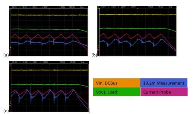
The inductor current measurement is important to determine the average current flowing through the converter. Due to optimization of the converter, the DS10.2m current sensor from Tell-i is a great candidate to use for being ultra-fast (bandwidth DC = 10 MHz), contactless, and with an isolated output. Results of the multi-phase megahertz board operating at 120 V, 6.78 MHz is shown below.
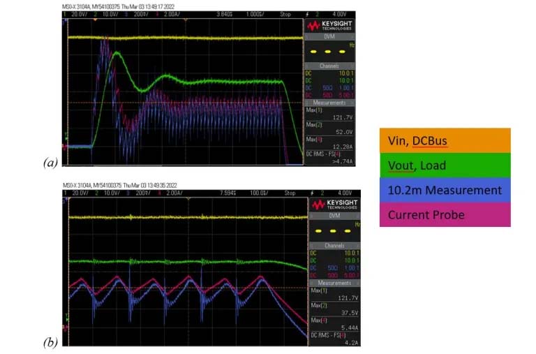
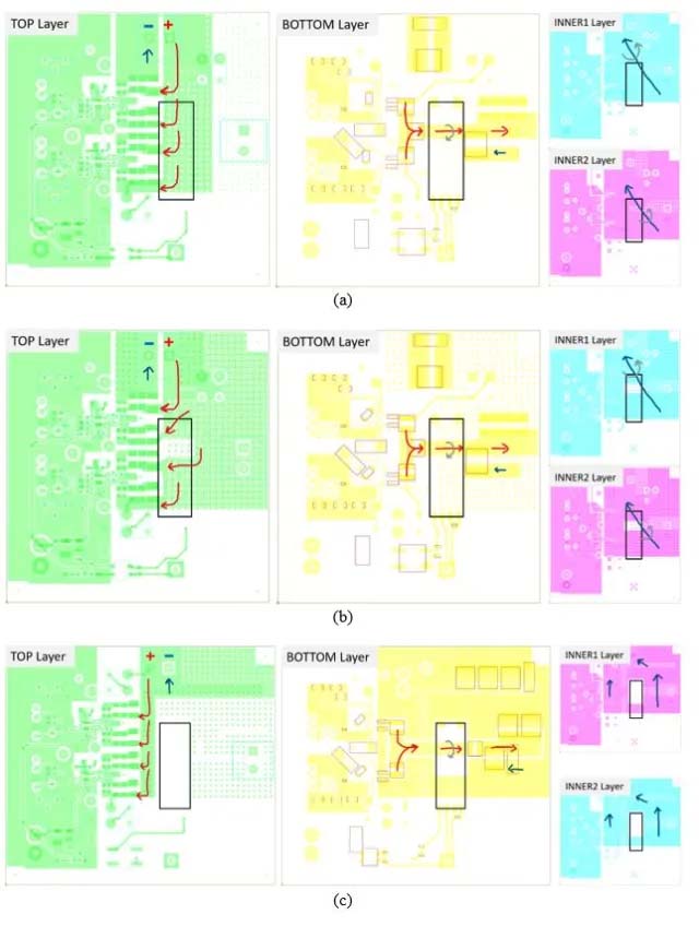
The DS10.2m current sensor (blue) is shown to follow the inductor current reference measurement (pink) at the 6.78-MHz frequency produced by the interleaved converters. To properly measure current, the current sensor must follow strict layout considerations to properly detect the current due to using magnetoresistive technology. Three different layouts are tested to verify the importance of layout using the current sensor. The changes are made around the effective area of the DS10.2m.
Layout consideration
Solely focusing on the area around the current sensor, the three layouts are examples of improper and proper layout placement. Clearance is specified as the effective area around the sensor with nothing but the current-carrying trace. Effective area is specified as the area around the current trace and current sensor. Figure 4 details possible current paths through the PCB layout. Red arrows indicate positive/forward current flow, blue arrows indicate negative/return current flow, and gray arrows indicate magnetic field direction.
Layout A contains no clearance over the effective area. While justified with the planes only containing ground/reference node, it is shown that there is a problem of current detection in the results based on shape and sensitivity of the sensor output. Layout A is not optimal.
Layout B contains some clearance over the effective area, allowing 50 mils of clearance around the current trace. Notice the effective area is imposed on all layers of the PCB to remove any possible interference of magnetic field. Results of Layout B show accurate measurement of beginning switching but fail to capture the result afterward because of interferences in return current. Layout B is still not optimal.
Layout C contains the minimal amount over the effective area, allowing 50 mils of clearance around the current-sensor package. Layout clearance is imposed on all layers as well, allowing only the current-carrying trace magnetic field in the effective area. Shown in the results, Layout C is optimal for clear and accurate measurement of the current. With no interference of return current, the current sensor detects only the current flowing through the current-carrying trace. Layout C is the most optimal layout but can be improved with more clearance around the entire sensor.
Conclusion
High-frequency converters can easily be achieved by proper and optimal layout placement. Higher frequencies above 1 MHz can also be achieved by using multi-phase techniques to double the effective switching frequency. To measure average current, Tell-i’s ultra-fast contactless current sensor, DS10.2m, can measure accurately if certain layout clearances around the sensor are followed. The isolated output is recommended and preferred from engineers to remove the need of thermal constraints and layout changes due to Hall or invasive current sensors.