Over the last few years, SiC MOSFETs have enjoyed a dominant role in high voltage (>600V) and high power applications. The advantages in thermal conductivity, high critical fields, much-improved switching efficiency, and the ability to form silicon dioxide on its surface have allowed key process, design and reliability improvements allowing its large-scale usage in some high-growth applications such as in EV’s for board chargers, traction inverters and DC to DC converters, PV inverters, motor control, transport systems and the power grid.
Back in the 1990s, most research on GaN was focused on the creation of blue and eventually white, LEDs and lasers. The direct bandgap of ˜ 3.4 eV, the ability to form quarternary layers with Al, In, P and quantum confinement through hetero-junction layers created through Metal-Organic CVD (MOCVD) laid the foundation for this. This work was then leveraged to take advantage of the high electron mobility and saturation velocity achieved in High Electron Mobility Transistors (HEMT) to create RF devices far superior to their Si counterparts. It is in this area of RF MMICs that the GaN PoweHEMT process and design technologies were significantly improved, and today, these form the backbone of some of the essential Communication, Radar and Electronic Warfare equipment, some with frequency ratings exceeding or at the RF X-Band spectrum (8.5 to 11 GHz).
The voltage range for these RF devices was typically in the <200V range. The lateral HEMT device has natural disadvantages over the Vertical V-DMOS typically used in SiC MOSFETs for HV device creation(see Figures 1 (a) and 1(b) for representative device cross-sections). High surface electrical fields in the lateral drift region between the gate and drain typically would limit the high voltage limits, and several advances in field plate technologies that shape/lower the electrical field would allow improvements in this rating.

Figure 1 (a) GaN Power HEMT device structure and Figure 1 (b) SiC VDMOS device structure
Table 1 lists some of the key material properties of SiC and GaN.
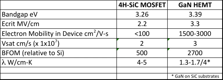
It should be noted that though the bulk SiC mobility as quoted in the literature is much higher (˜ 700 to 1000 cm2/V-s), the mobility obtained in the MOSFET is much lower, though to be due to trapping sites at the SiC/SiO2 interface. The mobility listed for the GaN Power HEMT is observed and reported on the 2 Dimensional Electron Gas (2-DEG) formed at the AlGaN/GaN interface, which forms the conduction channel of the device.
From this initial focus on RF devices, tremendous progress has been made on GaN transistors to deliver devices in the HV power FET range. Several companies such as Transphorm, ST Microelectronics, GaN Systems, Cambridge, Innoscience, GaN Power International, and Texas Instruments, to name just a few, offer devices at a 650V rating or higher. From a voltage perspective, this hits the sweet spot for several EV applications such as Level 2 On-Board Chargers (OBCs) and other applications long considered to be in the SiC domain. GaN offers lower terminal capacitances and improved mobility allowing device scaling and faster, more efficient switching. The lack of a p-n junction also allows for no reverse recovery loss from switching. Heat transfer and packaging then become key constraints, and a lot of research is now focused on improving this.
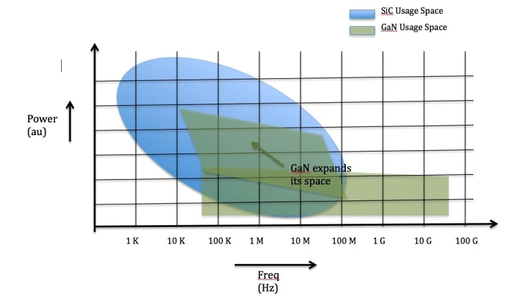
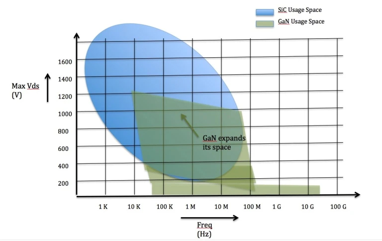
Figure 2 and Figure 3 below illustrate the expanding space of GaN in these applications.
The growth of GaN is typically done either on SiC or Si substrates. Buffer layers help relieve the stress from the lattice mismatch. RF GaN manufacturers have typically opted for the GaN on SiC approach to leverage SiC’s superior thermal capability for the high power density amplifiers. The Power FET industry has opted for the GaN on Si approach. The Si substrate offers a much cheaper approach and also offers an easier path for 200 mm wafer manufacturing. Innoscience has demonstrated this with their 8-inch GaN on Si Fabs in China.
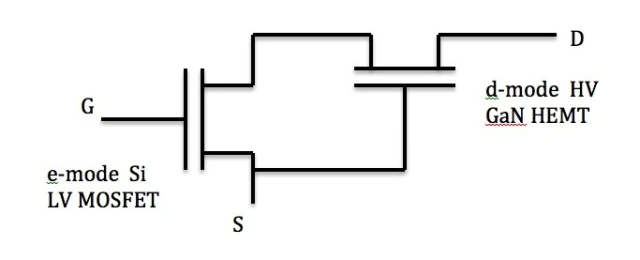
The GaN Power HEMT device is naturally a depletion mode device (or d-mode: normally on, would need a negative Vgs to turn off). For most Power FET applications, an enhancement mode (or e-mode: normally off, 0V should turn the device off) behaviour is essential. To this end, two different approaches have been used. On the one hand, barrier height modifications can be done using a p-type GaN or AlGaN gate, creating a depleted region underneath this layer that would create a normally-off device. This approach has been favoured by many to produce e-mode HEMT devices. Another approach has been to cascode an LV Si-MOSFET in series with the GaN device, as shown in Figure 4.
Tradeoffs exist between the two approaches. While the single e-mode device is simpler to use, makes paralleling devices less complex and offers superior capacitance and reverse recovery characteristics, the problem is that it is hard to achieve a threshold voltage much above 1.5V due to characteristics of the p-AlxGayN layer. This leaves the gate subject to switching noise and spurious device behaviour.
A much more robust gate is obtained with the cascode scheme, with Vt’s in the favoured≥ 2.5V range. The higher gate margin can enable a more straightforward gate driver.
To compare the device behaviour and the pros and cons of each approach, a parametric analysis is presented in Table 2 below. In this analysis, four devices are selected, two SiC MOSFETs and two GaN Power HEMTs. All four have a maximum Vds operation voltage of around 650V and a 25C Rdson rating of around 20 mOhms. The two GaN devices are labelled G1 and G2, while the SiC devices are S1 and S2. Devices S2 and G2, in addition, use the same package, so package-caused differences in some of the AC characteristics can be discounted in this case.
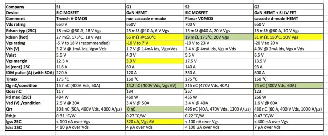
Parameters of concern are highlighted in yellow and favourable ones in green. It is immediately obvious that G1, with its single e-mode device, offers a key advantage of GaN, namely no reverse recovery charge Qrr. The poor gate margin, though, is also highlighted by the much higher Igss gate leakage. G2 on the other hand, has good gate margins, much like SiC, but with a corresponding increase in Qrr.
Generally, the lower gate charge Qg is highlighted in both GaN Power HEMTs. This can create a significant improvement in hard switching applications.
One clear disadvantage of GaN highlighted in Table 2 is the poor temperature coefficient of Rdson, with ≥ a doubling of the 25oC Rdson at 150C. It could also be argued that if the goal is to meet a certain 150oC Rdson, the GaN device would effectively have to be built with excess margin at 25oC, with a corresponding increase in die size and gate/output capacitance. The Rdson increase makes a more parallel device approach more critical. Paralleling GaN devices can present challenges due to the diverse parasitic components, especially in the cascoded arrangement. Integrated gate drivers with adaptive control can be a possible solution.