Reviewing some of the key device characteristics and applications of the more widely available GaN HEMTs along with the tradeoffs
GaN HEMT devices are at the forefront of creating new opportunities as well as replacing existing Si-based designs in a wide range of power conversion and power delivery applications. In this article, we will review some of the key device characteristics of some of the more widely available HEMTs and try to highlight some of the tradeoffs on each one.
The two most widely used approaches to GaN HEMTs for power applications are:
- e-mode: here the device could be formed with a p-GaN Schottky gate and result in a Vt of around 1.7V. Examples of this approach would be devices offered by GaN Systems, GaN Power International, Innoscience to name just a few. A notable exception to the relatively low Vt for e-mode devices is the offering from Cambridge GaN Devices which offers>2V e-mode devices through some innovative design approaches.
- A cascode approach where an LV Si MOSFET is essentially placed in series and creates the gate drive. Higher Vt’s can be achieved and Transphorm, Nexperia and others offer some examples of this.
E-mode devices have the advantage of using some of the intrinsic benefits of the GaN HEMT such as no reverse recovery loss due to lack of a p-n junction in the drain/source as well as simpler/lower parasitics from not having an additional device in series. One big disadvantage however is the poor margin for gate drive and a susceptibility to gate noise from the low Vth.
The cascode approach solves the poor gate margin of the e-mode and offers a more robust gate. This however is at the expense of potentially having higher switching losses from reverse recovery (Qrr) in the Si FET. Approaches taken to mitigate this are discussed later.
Some important application performance examples are listed below and a comparison is made between the two device approaches listed above
A. Hard/Soft Switching Characteristics of GaN HEMTs
Hard switching (HS): Examples include synchronous buck/boost converters and continuous conduction mode Totempole PFC AC/DC converters. Both conduction and switching losses affect the overall efficiency. In hard switching, turn-on losses can dominate due to reverse recovery and junction capacitance charge. The loss from input gate capacitance switching node charge/discharge also has a major role at high frequencies. The high dI/dt and dV/dt from high-frequency HS also place 3rd quadrant hard commutation requirements on the device which can be another loss component. Within this realm of HS, e-mode devices offer potentially lower losses due to the lack of the body diode and no Qrr. The factor to consider though is the low Vth of most e-mode devices, which are then prone to an oscillatory response under high-frequency HS and maybe need a negative gate bias to turn the device off completely. This can significantly complicate the gate driver circuitry.
Cascode devices with the higher Vth offer more Vgs margin and perhaps a simpler unipolar gate drive not needing negative turn-off voltages. The potential downside is the higher Qrr from the presence of the Si MOSFET. Solutions have been proposed to this such on Texas Instruments (TI) LMG352xR030-Q1 device which features a Si integrated gate driver with the GaN HEMT which drives the gate voltage of the GaN HEMT negative to turn it off in a switch-off event, while keeping the cascoded Si FET on, preventing the reverse loss of the Si device. Cascoded devices can also place design constraints on HS converters for the maximum reverse dI/dt at a switch-off transition [1]. This is from the gate of the GaN HEMT getting a high positive voltage from the recovery of the body diode within the cascoded Si MOSFET. This can reduce the transconductance of the GaN device and create more loss when operated at a higher than rated dI/dt.
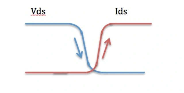
The dead-time loss component in the converter can also play a bigger role when a negative Vgs is needed in the off state as explained below. Since the GaN HEMT is a lateral n-channel without a p-body, reverse 3rd quadrant operation is essentially the HEMT operating backwards, i.e. a channel turn is required for the Vdg > Vth. This however depends on the state of the gate terminal during this, as shown in Fig 1.

In the case that a negative Vgs is needed to ensure full turn-off, as for some e-mode devices, these added Vgs will increase the effective Vsd. Conversely, if a positive Vgs could be applied during the 3rd quadrant operation it would lower the effective Vsd. The dead time loss in a converter Pdt ~ Vsd X Tdt, where Tdt is the dead-time. Compared to Si MOSFETs where the Vsd < 1V, GaN Vsd’s can be much higher, especially for e-mode HEMTs. A solution implemented in TI’s LMG352xR030-Q1 chip termed the ideal diode mode is where an adaptive gate drive is used to turn the GaN FET on when a negative Vds is sensed, moving the curve as shown in Fig 1 to the right and lowering dead time loss. The Si MOSFET in the cascoded structures presents a freewheeling diode with a lower turn-on voltage, hence presenting a net lower Vsd compared to the e-mode devices, which is useful in synchronous rectification, e.g. for motor drives.
Soft Switching (SS): Examples of these include Zero Voltage Switch (ZVS) such as an LLC auxiliary circuit that injects a resonant pulse that reduces to zero the voltage across the switch that has to be turned on, as shown in Fig 2.
Turn-on losses are therefore minimized. Since switching losses are minimized, it’s the conduction loss that can dominate SS topologies. A low output charge on the HEMT device (Coss) is also key as this lowers the peak magnetizing current. An analysis was done by Sojka, et al [2] compared HS and SS for the Transphorm TPH3205WSB cascode HEMT and concluded that ZVS is preferred when efficiency is the primary target and that SS performed better, especially at high switching frequencies. Böcker et al also showed that dynamic Rdson degradation could play a role in HS losses and SS was an advantage from this aspect [3].
B. Short Circuit Withstand Time (SCWT) for GaN HEMTs:
In motor drive applications power devices need to withstand overload or fault conditions that can create a situation in which the device is under both high voltage and high current conduction with the device in saturation. High temperatures can result in catastrophic damage. The power device and its gate driver need to work together to shut the device off, with 1us previously considered as a normal response time for this. Several studies on GaN HEMTs have reported much shorter SCWT times, thought to be from high current densities, especially in low Rdson devices. The SCWT drops dramatically as the Vds is raised up, with many studies showing < 500ns at a Vds ≥ 400V. A lower Vgs also helps, with the degradation in SCWT at high Vgs thought to be from hole accumulation under the gate [4]. A study to compare cascoded vs e-mode HEMTs [5] showed that the Idsat fall in cascoded devices from the short circuit (SC) thermal event was lower than for the e-mode devices which makes them less robust to the SC event. The larger percentage drop in Idsat on the e-mode devices from self-heating helps to strengthen its SC behavior.
An SCWT safe operating region was presented in a study [6] in which the authors also studies the effects of repeated SC events. The study found that although a single SC event at a Vds of 400V and Vgs 6V allowed for a large SCWT (>300us), repeated SC events only resulted in an SCWT of 20ns under these bias conditions. A significant de-rating of the Vds and/or Vgs was necessary to improve this time. The authors concluded that the heat confinement in the thin GaN channel layer created mechanical stress which caused the failure. A method for improving SCWT was been patented by Transphorm. This approach [7] dubbed Short Circuit Current Limiter (SCCL) effectively reduces the active region of the channel under the gate, thereby reducing Idsat and improving SCWT, though at a Rdson penalty that could range from 10-30%. When paired with a Desaturation Detection (DESAT) gate driver an 800ns detection was obtained at Vds = 400V and the full Vgs = 12V. Several fast SC detection methods have been proposed and it’s clear that this field will need significant development to validate the use of GaN HEMTs in motor control applications, especially at voltages ≥ 400V.
C. Packaging:
The cascode topology is more robust for gate voltage and is hence more immune to parasitic inductance/capacitance to a certain extent than the e-mode counterparts. Some cascode devices have been packaged in thermally robust packages like the TO-247. E-mode devices to a large degree are more prone to gate noise issues and careful consideration of package-related parasitics has to be done. As a result, a lot of the offerings for this have been in leadless planar packages. Technology development at the package level is therefore essential to assure the high thermal sinking needed in these high power density devices. Having a Kelvin source connection also allows for more accurate gate control without the common source inductance. GaN Systems has come up with an innovative GaNPX® package that offers low thermal resistance.