When it comes to implementing custom logic, there are two names that stand out: ASICs (Application-Specific Integrated Circuits) and FPGAs (Field-Programmable Gate Arrays), both are used in building complex digital circuits. Despite the similarity in their circuit designs, their characteristics, use cases, performance metrics, and design methodologies are worlds apart. If someone wants to make informed decisions about hardware development, understanding the differences between ASICs and FPGAs is a must.
.png)
.png)
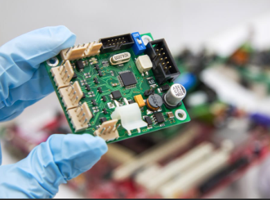
ASICS (Application-Specific Integrated Circuit):
As the name suggests, ASICs are custom-designed silicon chips built for only one specific task or application. They are built to focus on very high speed, lower buffers, and fewer features. They are designed with the sole purpose of providing as much throughput as possible.
Key Features of ASICs:
● Built for a specific function.
● Better performance with lower power consumption.
● Once made, the logic is fixed and cannot be changed.
● Expensive to design and manufacture but cost-effective when produced in large numbers.
Types of ASICs
ASICs can be classified into several types based on how customizable they are and how they are developed:
1. Full-Custom ASICs
In full-custom ASICS, every part of the chip is designed from scratch because of which these are expensive and time-consuming to develop. Full-custom ASICS provide the best performance, efficiency, and cost-effectiveness.
2. Semi-Custom ASICs
Semi-custom ASICs use pre-designed logic cells called "intellectual property (IP)" cores, which speed up development while still allowing a high degree of customization.
Design and Development Process:
Designing an ASIC is a time-consuming, complex, and expensive process involving multiple specialized stages to make sure that the final chip meets the performance, power, and area requirements.
The first phase of the process is defining function performance levels and needs. RTL (Register Transfer Level) code is written using Hardware Description Languages (HDLs) like Verilog or VHDL, describing how data will move and be processed inside the chip.
The RTL code is converted into a gate-level netlist, which is made up of logic gates and flip flops and is used to determine where each logic gate and memory block will be placed on the chip. Routing connects all gates with physical wires. Then, test structures like scan chains and BIST circuits are inserted to make sure that the chip can be tested once it is manufactured.
The final design files are then sent to the fabrication facility (fab). This is called "tape-out", which means that the chip is ready to be physically manufactured in a semiconductor fab (e.g., TSMC, Intel). The entire process can take months or even years and costs millions of dollars.
Cost
ASICs require a substantial upfront cost, mostly because of the NRE (Non-Recurring Engineering), which includes design, verification, testing, and especially fabrication—one of the most expensive parts of the process. Creating custom photomasks and accessing a fabrication facility can cost millions of dollars. However, once the chip is fabricated, the per-unit cost becomes very low, especially at high volumes.
Performance
ASICS are built specifically for a particular task, which is why they give the highest possible performance. Every gate and wire in the design is placed and optimized for speed. There's no extra overhead from routing or configurable logic, and timing is also tightly controlled.
Power Efficiency
Being custom-built gives ASICs an edge when it comes to power efficiency since engineers can design them to use the minimum required logic and power, optimizing both dynamic and static power at every stage, making ASICs ideal for battery-powered and energy-sensitive devices such as smartphones, wearables, and IoT devices.
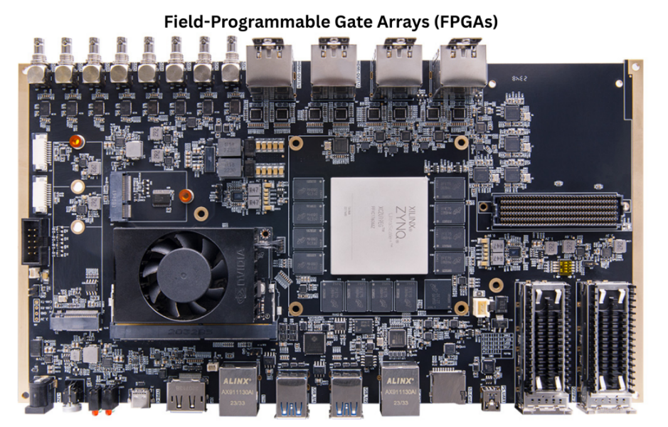
FPGA (Field-Programmable Gate Array)
FPGAs are reprogrammable and versatile hardware platforms designed to suit different needs and wants. They are made up of configurable logic blocks (CLBs), interconnects, and I/O blocks, allowing designers to customize their logic by writing configuration files according to the needed functionality.
 C
C
Key Features of FPGAs
● Logic can be modified after manufacturing.
● Perfect for testing new designs.
● Lower performance than ASICs, but flexible.
● Less power-efficient than ASICs.
Types of FPGAs
FPGAs vary by architecture, features, and application suitability:
1. SRAM-Based FPGAs
SRAM-Based FPGAs use static RAM cells to store configurations. These configurations are sensitive to radiation effects and are capable of corrupting the design and changing the FPGAs' intended function. SRAM-based FPGAs are very volatile and must be reloaded from external memory on power-up, which allows devices to reconfigure completely.
3. Flash-Based FPGAs
Flash-based FPGA stores configuration in non-volatile flash memory. Each cell has a floating-gate transistor, which defends against radiation effects since the radiation cannot generate enough charge to affect the configuration state. Flash-based FPGAs become live at power-up and retain logic after power-off. Two transistors are used by the flash memory cells, which results in improved logic density, smaller delays, more security, and increased power efficiency.
4. Antifuse-Based FPGAs
Antifuse-based FPGAs are also non-volatile but are one-time programmable (OTP), resulting in prototyping challenges. These FPGAs are very secure, have high resistance to radiation, and are used in aerospace, defence, and critical systems. Antifuse-based FPGAs, as compared to similar SRAM devices, also consume less dynamic and static power.
Design and Development Process
FPGA development is much faster and more flexible than ASIC design. Instead of physical manufacturing, you configure existing programmable hardware.
The first step is to define the functions and performance requirements for the FPGA. The RTL code is written in Verilog or VHDL, defining the behavior of logic circuits. The RTL is simulated to check the logical correctness, after which the RTL code is converted into logic gates using FPGA synthesis tools, which map the design onto the available logic elements (LUTs, flip-flops) inside the FPGA.
The logic is then placed on physical resources like CLBs (Configurable Logic Blocks), DSP blocks, and memory. Routes (interconnects) are established between components, and then the timing constraints are analyzed and adjusted. The output is a bitstream file, which is then loaded onto the FPGA chip using a programmer or JTAG cable. This loop can be completed in just a few days or even hours.
Cost
FPGAs don’t have any fabrication cost since they use pre-manufactured programmable chips. They have low upfront costs and are excellent for projects with limited budgets, small production runs, or development timelines that are not very lengthy.
Performance
FPGAs are inherently slower because their architecture includes programmable interconnects, which introduce latency and reduce the maximum achievable clock speed. Although FPGAs have improved significantly over the years, they still lag behind ASICs.
Power efficiency
FPGAs use more power because of their programmable nature. The configuration logic, routing overhead, and general-purpose architecture need more power to perform the same task compared to an ASIC. That said, some vendors offer low-power FPGA families that target power-sensitive applications but still can't match ASIC efficiency.
To get the best Lattice FPGAs for your systems, check out JAK Electronics, the best in the game.
Comparison Table
|
Feature |
ASIC |
FPGA |
|
Customization |
Fixed |
Reprogrammable |
|
Types |
Full-custom, Semi-custom, Gate Array |
SRAM, Flash, Antifuse |
|
Performance |
Very High |
Moderate |
|
Power Efficiency |
Excellent |
Moderate to Poor |
|
Development Cost |
Very High |
Low to Medium |
|
Per Unit Cost |
Low (in bulk) |
High |
|
Time to Market |
Long |
Fast |
|
Design Flexibility |
None after fabrication |
High |
|
Reliability |
Very High |
Moderate to High |
|
Security |
Strong |
Varies (Antifuse > Flash > SRAM) |
|
Ideal For |
Mass production, stable design |
Prototyping, evolving applications |
Conclusion
In many modern systems, both technologies can coexist. For example, a design can be built on an FPGA and then shifted to an ASIC for large-scale production. Alternatively, FPGAs may be used with ASICs for better configurability or adaptability in hybrid systems. Ultimately, both ASICs and FPGAs play important roles in hardware development. Understanding their strengths and weaknesses makes it easier for you to select the right technology.