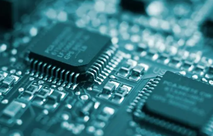
What is ASIC Chip
ASIC chips are Application-Specific Integrated circuits that are custom-designed for a specific task or system and are more specialized than general-purpose processors or multifunctional chips. Through custom design and manufacturing, ASIC chips can provide higher performance and smaller area at the same power consumption. In addition, ASics reduce the number of parts and assembly costs, improving the efficiency and reliability of the entire system.
ASIC chips are manufactured through a photolithography process in which transistors and other components in a custom layout are etched onto silicon wafers. This layout enables functions ranging from simple logic gates to complex digital signal processing circuits. While the manufacturing process for ASics is time-consuming and expensive, including multiple steps such as mask fabrication, wafer fabrication, and packaging, the unit cost decreases significantly as production volumes increase.
Asic Chip Design
The ASIC chip design process consists of several stages. The first step in the ASIC design process is to define system requirements and specifications, including functions, performance goals, power consumption limits, and more. Designers create detailed documentation according to the specification as a guide for ASIC design. The second step is the design phase, which translates the system specification into the ASIC layout. Refinement through logical integrated design, converting high-level descriptions into gate level netlists, and then optimizing the netlists' area, power consumption, and performance. Wiring then connects the grid and components on the silicon wafer. The second step is particularly important because it cannot be changed after manufacturing, so it is important to pay great attention to this design stage. The third step is the verification phase to ensure that the design is compliant and correct. Once the design has been validated, it moves on to the fourth manufacturing phase, which involves manufacturing the ASIC chip. The final step is to conduct tests to ensure the ASIC's performance and reliability. Finally, the ASIC chip confirmed by the test can be put into use in the electronic system.
Here is a useful video to help you better understand the Asics design:
Asic chip features
(1) Advantages:
① Area advantage: ASIC chips are designed to avoid redundant logic units, processing units, registers, storage units and other architectures, and are built in the form of pure digital logic circuits, which is conducive to reducing the chip area. For small area chips, more chips can be cut out of wafers of the same specification, which helps enterprises reduce wafer costs.
② Energy consumption advantages: ASIC chip unit computing power consumption is lower than CPU, GPU, FPGA, such as GPU per computing power average consumption of about 0.4 watts of power, ASIC unit computing power average consumption of about 0.2 watts of power, more to meet the new smart home appliances to limit energy consumption.
③ Integration advantage: Due to the custom design, ASIC chip system, circuit and process are highly integrated, which helps customers to obtain high-performance integrated circuits.
④ Price advantage: Affected by the characteristics of small size, high running speed and low power consumption, the price of ASIC chips is much lower than that of CPU, GPU and FPGA chips. At present, the average price of ASIC chips in the global market is about $3, and if the mass production scale is reached in the long term, the price of ASIC chips is expected to continue to decline.
(2) Disadvantages:
① ASIC chip customization degree is high, the design and development cycle is long, the finished product needs to do physical design and reliability verification, the market time is slow.
② ASIC chip has high dependence on algorithm. Artificial intelligence algorithm update iteration at high speed, resulting in higher ASIC chip update frequency.
③ Due to the high degree of customization of ASIC chips, the research and development cycle is relatively long, which expands the risk of ASIC finished products being eliminated by the market.
Asic chip Applications
- Communication field: In the field of communication, ASics are widely used in base stations, routers, optical communication and other scenarios. These applications require high levels of performance, reliability and power consumption, and ASics can meet these needs.
- Data centers: Data centers have extremely high requirements for computing and storage capabilities. The high efficiency and low power consumption of ASics make them ideal for building high-performance servers.
- Internet of Things: iot devices need to process large amounts of data while ensuring low power consumption. With its high efficiency and energy saving characteristics, ASIC has a wide range of application prospects in the field of Internet of Things.
Types of ASIC chip
ASIC chips can be classified according to different design and manufacturing methods, mainly including the following types:
Full Custom ASIC (Full Custom ASIC) : A full custom ASIC is a chip that is custom-designed and manufactured entirely according to specific application requirements. Each circuit element and connection is precisely laid out and wired according to design requirements, with the highest performance and power efficiency, but also with the highest development and manufacturing costs.
Standard Cell ASIC (Standard Cell ASIC) : Standard cell ASics use a pre-designed Standard Cell Library to build circuits, and designers can select and combine standard cells to implement functions as needed. Compared to fully custom ASics, standard unit ASics have lower development costs and manufacturing time, but slightly less flexibility.
Gate Array ASIC (Gate Array ASIC) : A gate array ASIC is a type of chip that falls between a fully customized ASIC and a standard unit ASIC. It features a pre-arranged array of logic gates, which designers can customize as needed. The design flexibility of gate array ASics is somewhere between fully custom and standard cell ASics, and the cost and performance fall somewhere in between.
Hybrid ASics: Hybrid ASics combine standard cells, gate arrays, and other customized components to strike a balance between design flexibility and performance. This type of ASIC is often used in application scenarios that require custom functionality but require lower development costs.
ASIC chip VS FPGA
Compared with an FPGA, the circuit structure of an ASIC is fixed and is usually used in mass production and Specific Application scenarios. Fpgas, on the other hand, are programmable and can be configured and reprogrammed in the field as needed, suitable for small batch production and flexible design needs.
The FPGA versus ASIC debate revolves around the tradeoff between design flexibility and performance optimization. But there are several parameters to consider when choosing between the two.
|
ASIC |
FPGA |
|
|
Performance |
Asics are tailored for specific functions, so they can be designed to maximize efficiency and speed, resulting in better performance for target applications. |
Fpgas are more flexible and reprogrammable, but this flexibility comes at the cost of performance. The programmable nature of FPgas imposes overhead in area, power consumption, and performance because configurable logic blocks and interconnects are less efficient than custom-designed components in ASics. |
|
Energy consumption |
Asics are designed for specific applications and are highly optimized in terms of power consumption. By minimizing the number of active components and customizing them to meet target functions, ASics can achieve lower power consumption than general-purpose processors and FPgas. |
Fpgas typically have a lower clock rate, which can lead to increased dynamic power consumption for some applications. Fpgas, on the other hand, have relatively high power consumption due to their programmable nature. The FPGA's configurable logical blocks, interconnects, and other resources provide flexibility, but also result in high power consumption. |
|
cost |
The cost is higher and not suitable for small companies or projects with limited budgets. The manufacturing process is complex and has a certain impact on the total project cost and delivery time. |
The overall cost is low, but the unit cost is higher than ASIC and is not suitable for mass production. Fpgas can be purchased off the shelf and reprogrammed as needed, reducing manufacturing complexity and shortening lead times. |
|
flexibility |
Asics, as custom-designed devices, have limited design flexibility after manufacturing is complete. Any changes to ASIC functions or characteristics require new design and manufacturing processes, which can be time-consuming and costly. |
Due to their programmable architecture, FPgas offer a high degree of design flexibility. |
In SUMMARY:
- In terms of performance, ASics are the preferred solution for applications that require high efficiency and speed, while FPgas are the more appropriate choice for applications that require rapid prototyping, design flexibility, or adaptation to changing conditions.
- In terms of power consumption, for those applications that require the lowest power consumption, ASics are the preferred solution, while for applications that require design flexibility or adapt to ever-changing applications, FPgas are the more appropriate choice.
- In terms of cost, it is necessary to consider the trade-offs between the specific requirements of the application, upfront investment, unit cost and design flexibility. For high volume production or applications requiring minimum unit costs, ASics may be preferred. For small batch production or projects with rapidly changing needs, FPgas are a more suitable choice.
- In terms of design flexibility, ASics may be preferred for applications that require the highest level of optimization and fixed functionality. Fpgas are better suited for applications where requirements may change over time or the ability to update functionality is important.
ALSO READ: FPGA vs CPU: Detailed Comparison Between FPGA and CPU