Overview: This article discusses the use of additive manufacturing technology in power electronics converters, including the seven categories of 3-D printing technologies. In-depth analyses of a few technologies and their benefits and drawbacks are discussed.
Additive manufacturing technology is also recognized as a way to realize autonomous manufacturing since many intermediate processes can be removed during the additive manufacturing process. Additive manufacturing, sometimes called 3-D printing, is a technique for fusing materials to create parts.
Classification of Additive Manufacturing Techniques
In 2010, the American Society for Testing and Materials (ASTM) divided different 3-D printing technologies into seven groups: binder jetting, directed energy deposition, material extrusion, material jetting, powder bed fusion, sheet lamination, and vat photopolymerization.
These seven categories do not imply that there are just seven ways to do additive manufacturing. Instead, they stand for a collection of additive manufacturing methods. Different 3-D printing technologies are included in each class, each with its own benefits and drawbacks regarding price, material qualities, tolerance control, and printing speed. The additive manufacturing process uses the following techniques when applied to power electronics converters.
VAT photopolymerization: SLA
Stereolithography (SLA) printers are typically used to manufacture nonmetal polymer structures for electrical cross-sections. A computer-controlled laser beam pointed at the surface solidifies the first layer's design. The platform descends according to the thickness of the layer following the first layer's solidification. The second layer is cured using the same technique on top of the first, and this cycle is repeated throughout the entire component.
In addition, digital light projection (DLP) illumination can be used instead of scanning lasers. With this method, the entire 2-D pattern of each layer may be projected onto the glass plate, curing the resin in one step. Figure 1 displays two alternative SLA system types with various building orientations and illumination setups. The heat sinks for the power electronics converters have been printed using this method. SLA can also be used to create the substrate for electrical circuits and the supporting framework for passive components.
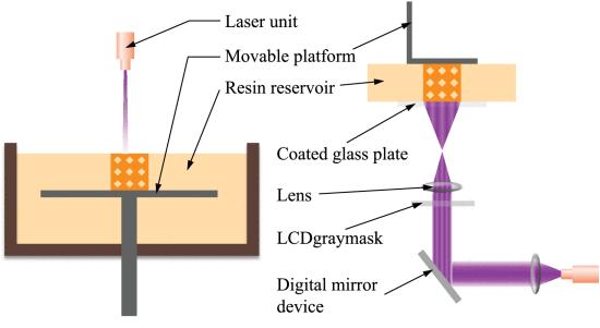
Figure 1. Schemes of two types of SLA systems. Image used courtesy of IEEE Journal of Emerging and Selected Topics in Power Electronics
Powder bed fusion: SLM and DMLS
Selective laser melting (SLM) and direct metal laser sintering (DMLS) are typically employed for building metal or alloy parts for electronic systems. These two construction methods use extremely similar methods. SLM serves as an illustration of how the process works, which is shown in Figure 2. It begins with a base plate in the building chamber covered with a thin layer of powder. A high-energy-density laser is then used to fuse and sinter the powder in the chosen area to create the initial cross-section.
A new layer of powder is applied over the first layer using a wiper blade or a roller as the platform descends after this stage. After that, a new layer is fused and placed on top. The process is repeated until the 3-D model is finished. SLM and DMLS follow similar processes. The primary distinction between them is that the metal powder is completely melted in the SLM process using a laser, but in the DMLS process, only some constituents reach a complete melt state.
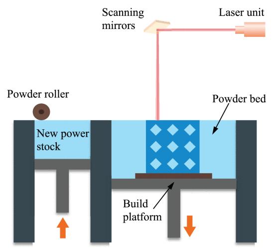
Figure 2. Schematic of the SLM building process. Image used courtesy of IEEE Journal of Emerging and Selected Topics in Power Electronics
DMLS and SLM are good options for producing metal structures because they offer high metal forming quality and good metal performance. Several metal and alloy parts, including 3-D-printed windings, magnetic components, and metal heat sinks, are created using these processes in power electronics converters.
Material extrusion: FDM
Fused deposition modeling (FDM) is a simple and affordable process that sources its building materials from thermoplastic filaments, most frequently acrylonitrile butadiene styrene (ABS) or polylactic acid (PLA). The two materials used in the FDM process are fed from spools into a heating section and heated to the semiliquid phase, together with any necessary building and support components. The semiliquid substances are extruded through extrusion nozzles, printed onto the build platform, and formed into the required shape, as shown in Figure 3.
The extrusion head then rises by a layer thickness to repeat the process of depositing subsequent layers on top of prior layers until the entire product is fully produced. This procedure can be widely applied in power electronics domains and other electrical areas because of how straightforward it is. In this method, conducting elements of passive components and electric circuits can be created using metal-based filaments, while supporting structures for passive devices and jet coolers can be created using plastic filaments.
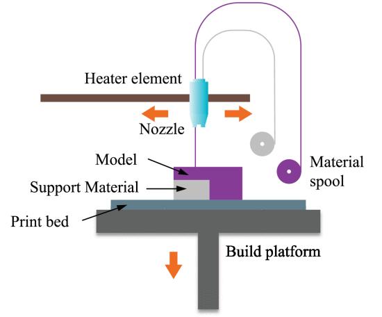
Figure 3. Schematic of the FDM process. Image used courtesy of IEEE Journal of Emerging and Selected Topics in Power Electronics
Material jetting: AJP
The Optomec company's mesoscopic integrated conformal electronics (MICE) program led to the development of the aerosol jet printing (AJP) process, a noncontact printing method. This approach was developed primarily for electronic printing purposes, unlike other additive manufacturing processes. Figure 4 illustrates the practical ideas and important actions of AJP. To create a thick aerosol stream, the conductive ink is placed into an ultrasonic atomizer or into a pneumatic aerosol generator, where it is aerosolized via ultrasonication.
The mist is delivered into the virtual impactor by inert molecules like nitrogen gas, where the extra carrier gas is eliminated to increase the aerosol droplet density. The flow deposition head receives the pressurized aerosol droplets after that. Within the deposition nozzle, the aerosol is focused by an annular flow of sheath gas into a high-velocity stream of aerosol droplets projected onto the substrate to create delicate features.
The wet printed ink is converted into solid patterns to obtain their ultimate qualities. A post-processing technique for increasing the conductivity of metallic traces is thermal sintering. This method makes use of the printer's six-axis precision motion control technology to produce freeform patterns on a variety of complicated surface shapes. Its industrial applications are, therefore, numerous. The conductive traces of electrical circuits, antennas, passive components, and thin-film transistors can be printed using AJP in electronics.

Figure 4. Functional principle of an aerosol jet printing system. Image used courtesy of IEEE Journal of Emerging and Selected Topics in Power Electronics
The ability of AJP to connect chips and substrates instead of using traditional packaging methods has possible benefits for power semiconductors, even though it is not necessary to use these applications for power electronics converters.
Summarizing the Key Points
- Additive manufacturing technology has the potential to revolutionize the power electronics industry by enabling autonomous manufacturing and reducing intermediate processes.
- The seven categories of 3-D printing technologies offer a range of benefits and drawbacks in terms of price, material qualities, tolerance control, and printing speed.
- The four primary techniques used in power electronics converters - VAT photopolymerization, powder bed fusion, material extrusion, and material jetting - each have unique advantages and applications.
- Material jetting is a promising technique for interconnecting chips and substrates in power semiconductors, offering potential advantages over conventional packaging methods.
- As additive manufacturing technology continues to evolve and improve, it is likely to see even more innovative applications in the field of power electronics converters in the years to come.
This blog post is part of a full research article from the IEEE Journal of Emerging and Selected Topics in Power Electronics.
The featured image is courtesy of Midjourney.