Failure models of SiC JFETs and MOSFETs in short-circuit events portray that failure current is higher than the rated current of power devicea
Silicon carbide power devices have emerged as a promising technology for the growing interest in reducing energy consumption and operating under high-switching–frequency applications. SiC can also sustain high operating temperatures, making it a suitable candidate for the industrial environment. The availability of wide-bandgap semiconductor devices has enabled engineers to design power-electronic systems to meet specific application requirements.1 Along with SiC, gallium nitride also falls in the wide-bandgap category. Some of the major factors to be taken into account before designing any power system are cost, efficiency, power density, complexity, and reliability.2
SiC MOSFETs are usually susceptible to damage as a result of short-circuiting events because of the fast switching speeds and low on-state resistance.3 A team of researchers affiliated with the School of Electrical and Information Engineering at Anhui University of Technology have presented failure models of SiC devices in short-circuit events in two commonly used power devices: the SiC MOSFET (N-channel enhancement SiC MOSFET from Cree) and the SiC JFET (normally on SiC JFET from Infineon).4
Developing failure models for SiC transistors in short-circuit events
In a paper proposed by Wang et al., the study shows that under short-circuit events, the failure current is higher than the rated current of the power device.5 This means the leakage current contributes to the failure current, and to verify this, technology computer-aided design (TCAD) simulation is used. The current component of the SiC JFET and SiC MOSFET depicts the hole current density in both the SiC transistors. Analyzing the executed file, we can conclude that the high-density hole current flows through the p-n junction between the N-drift region and P-base region of the transistors. “TCAD simulation has also shown that for the SiC MOSFET, high-concentration carriers assemble on the top of the JFET region; a fraction of them inject into the gate oxide and form the gate leakage current under the stress of high temperature and high electric-field strength,” the team explains.

Figure 1: Distribution of hole current density in the SiC JFET (left) and SiC MOSFET (right) before failure
The schematics of the failure models of the SiC JFET and SiC MOSFET are designed considering the introduction of the leakage current. The structure in the dotted boxes is part of the traditional circuit models and the additional current component IDS_LK connected in parallel with the channel current ICH is the leakage current across the p-n junction between the N-drift region and the P-base region of the transistors. For the study, the researchers explicitly note that the gate leakage current for SiC JFET is not considered for no voltage bias on the gate to turn the device on.
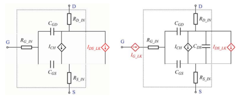
The expressions for the leakage current through the p-n junction consist of the thermal generation current Ith, avalanche current Iav, and diffusion current Idiff. However, for the leakage current in the gate oxide, several methods have been proposed of which the team has considered the Fowler-Nordheim (FN) tunneling and Poole-Frenkel (PF) emission. So the currents IFN and IPF are considered to contribute to the leakage current of the SiC MOSFET gate oxide.
For circuit simulation of the SiC MOSFET, the SPICE Level 1 model based on the Shichman-Hodges physical model is used to describe the three modes — cutoff region, linear region, and saturation region — while for the SiC JFET, the Shockley physical model is used. Typically, in the short-circuit events, the charge carriers in the channel are affected by the higher current stress and are heated to a higher temperature with respect to the normal switching state. Due to this, the accurate mobility model of channel carriers is important to understand the carrier behavior on the effect of short-circuit performance of the transistors.
Verification of the failure models
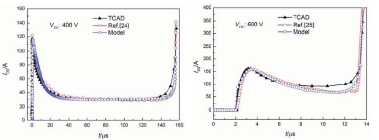
Verification of the developed failure models of the SiC JFET and SiC MOSFET is done under short-circuit fault circumstances, with the figure showing a comparison of the failure currents obtained from the models and the results presented in the paper.6,7 The results show that under 400-V DC voltage, the short-circuit failure time (tSC) for the SiC JFET is 150 μs, and for the SiC MOSFET under 600 V, DC voltage is 13 μs. (Editor’s note: Figure 3 shows Refs. 24 and 25, considered as References 6 and 7 in this article.)
“The carrier mobility dependent on temperature and electric-field strength is necessary to accurately develop the failure model of the SiC power device,” the team notes. “Furthermore, by changing the combination mode of three current components of IDS_LK, a conclusive result can be achieved that ITH determines whether the developed model can simulate the failure of the device or not. So the thermal generation current during short-circuit fatefully dominates the failure effect.”

The verification under short-circuit fault circumstances is shown by the schematic diagram with VDC as the DC-link voltage, RS as the stray resistance of the circuit loop, RG as the gate resistance, and DUT as the device (SiC JFET or SiC MOSFET). The two failure modes are demonstrated in the figure, showing the red curves as the first failure mode and blue as the second failure mode. Some of the parameters noted are that the failure time of the SiC JFET is much longer than that of the SiC MOSFET, and the saturation current of the SiC JFET is lower than that of the SIC MOSFET. The reason for these changes is the temperature-dependent coefficient of carrier mobility.
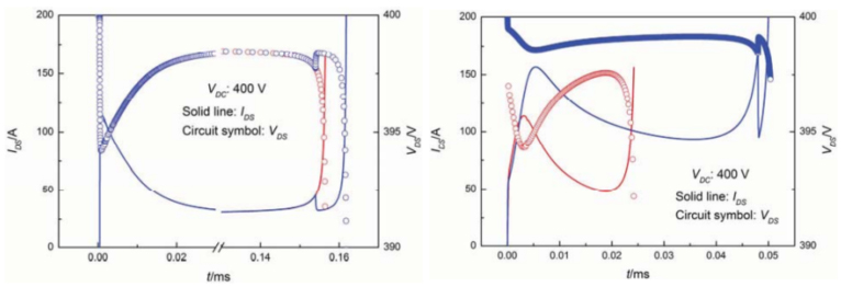
“For immediate failure, the SiC JFET exhibits better short-circuit capacity than the SiC MOSFET, and the failure time and critical failure energy for the SiC JFET are both higher than that of the SiC MOSFET,” the team concludes. “For delayed failure, under lower DC-link voltage, the failure time of the SiC JFET is much longer than that of the SiC MOSFET; however, for higher DC-link voltage, the difference of failure time for the two SiC transistors seems small.”
The research paper is published in the 2018 1st Workshop on Wide Bandgap Power Devices and Applications in Asia (WiPDA Asia) and is available under closed-access terms.