The Raspberry Pi 5 has arrived, bringing with it powerful upgrades for you over its predecessor, the Raspberry Pi 4. With enhanced processing power, improved I/O capabilities, and greater support for advanced projects, the Raspberry Pi 5 is a game-changer for you as hobbyists and as seasoned electronics makers.
To truly harness the power of the Raspberry Pi 5, you need to understand how to use its GPIO (General Purpose Input/Output) pins effectively. That’s where we come in! Our Complete Raspberry Pi 5 Pinout Guide is designed to help you get started with your next big project.
In this all-in-one resource, we cover everything you need to know about the Raspberry Pi 5’s pinout, including:
· Learn about the new capabilities of the Raspberry Pi 5 that will take your projects to the next level.
· See how others are leveraging the power of the Raspberry Pi 5 for cutting-edge projects.
· Easily reference pinout details with clear and accessible tables.
· Discover how to use the GPIO pins for a wide range of purposes, from simple tasks to complex innovations.
Whether you're building a new project or upgrading an existing one, our guide ensures you can unlock the full potential of the Raspberry Pi 5. Don’t miss out and get started now.
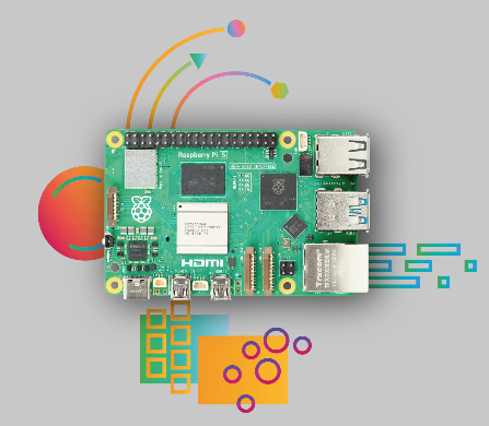
Raspberry Pi 5 (Source: Raspberry Pi Foundation)
What’s New in Raspberry Pi 5?
Before you move into the Raspberry Pi 5 Pinout details, let’s briefly go over what's new in it. The Raspberry Pi Foundation has made some important upgrades to this version. Some of the key upgrades are:
1. They have added a quad-core Cortex-A76 processor to the Pi 5. It is significantly faster than its predecessors Quad-core ARM Cortex-A72 processor used in Pi 4. It has made it suitable for more demanding applications like live media streaming or AI experiments without lagging issues.
2. The Raspberry Pi 5 now supports two 4K displays simultaneously. This will now provide better support for visual projects or home theatre setups.
3. There are additional USB Ports in Pi 5 as compared to Pi 4. With 2 USB 3.0 and 2 USB 2.0 ports, you can now have more connectivity options.
4. The power management has been improved as well. You can use more peripherals without worrying about the excessive power it draws.
These upgrades are great to learn but to unlock the potential of your Raspberry Pi 5, you need to understand how to use its pins correctly. So, we have come up with the details in this article.
The Basic of Raspberry Pi 5 Pinout
The GPIO pinout on the Raspberry Pi 5 is largely similar to previous models, making it easier to transition. If you are already familiar with earlier versions of the Pi, you can quickly lean forward to Pi 5. The GPIO header on the Pi 5 has 40 pins, which are divided into the following categories:
1. Power (5V and 3.3V) pins for powering external components.
2. Ground (GND) pins for providing a common ground.
3. GPIO Pins to be configured as input or output for controlling various devices.
4. Special Functions pins support UART, SPI, I2C, PWM, and other communication protocols.
Pinout Table
Below is a breakdown of the 40 pins, grouped by function:
|
Pin |
Function |
Pin |
Function |
|
1 |
3.3V |
2 |
5V |
|
3 |
GPIO 2 (SDA) |
4 |
5V |
|
5 |
GPIO 3 (SCL) |
6 |
GND |
|
7 |
GPIO 4 |
8 |
GPIO 14 (TXD) |
|
9 |
GND |
10 |
GPIO 15 (RXD) |
|
11 |
GPIO 17 |
12 |
GPIO 18 |
|
13 |
GPIO 27 |
14 |
GND |
|
15 |
GPIO 22 |
16 |
GPIO 23 |
|
17 |
3.3V |
18 |
GPIO 24 |
|
19 |
GPIO 10 (MOSI) |
20 |
GND |
|
21 |
GPIO 9 (MISO) |
22 |
GPIO 25 |
|
23 |
GPIO 11 (SCLK) |
24 |
GPIO 8 (CE0) |
|
25 |
GND |
26 |
GPIO 7 (CE1) |
|
27 |
GPIO 0 (ID_SD) |
28 |
GPIO 1 (ID_SC) |
|
29 |
GPIO 5 |
30 |
GND |
|
31 |
GPIO 6 |
32 |
GPIO 12 |
|
33 |
GPIO 13 |
34 |
GND |
|
35 |
GPIO 19 |
36 |
GPIO 16 |
|
37 |
GPIO 26 |
38 |
GPIO 20 |
|
39 |
GND |
40 |
GPIO 21 |
* Be cautious when connecting components. While the Pi 5 operates at 3.3V logic on its GPIO pins, certain peripherals may use 5V, and applying 5V directly to the GPIO could damage the board.
** Many GPIO pins can serve multiple functions. For instance, some pins support I2C, SPI, or PWM (pulse-width modulation). You can configure them based on your project's needs.
Ready to get started? Grab your Raspberry Pi 5 and dive into the world of limitless possibilities today!
Understanding the Raspberry Pi 5 Pinout
Please do not take that the Raspberry Pi 5 pinout is just about connecting devices to GPIO pins. Each pin has a technical functionality packed into it with respect to data transmission, signal processing and power management. That is why, each pin needs to be calibrated and configured accordingly.
GPIO Pin Configuration and Modes
As previously mentioned, it has the same 40-pin configuration as Raspberry Pi 4. It has been chosen for the functional blocks and their locations on the GPIO pins have been chosen to match user-facing functions as previously used by them on the 40-pin header of a Raspberry Pi 4 Model B.
Among the 40 pins, the Raspberry Pi 5 has 28 multi-functional General-Purpose Input/Output pins available to implement the standard Raspberry Pi 40-pin GPIO connector. These pins need to be configured for different purposes. Different projects and requirements work on specialized configurations
The pins are in a single electrical bank (VDDIO0). The GPIO bank (IO_BANK0) can be powered from 1.8V or 3.3V, but interface timings have been specified at 3.3V. Each pin can be controlled directly by software, or by a number of other functional blocks.
The GPIO bank supports the following functions:
· 5 × UART
· 6 × SPI
· 4 × I2C
· 2 × I2S - 1× Clock Producer instance, 1× Clock Consumer instance.
· RIO - Registered IO interface
· 24-bit DPI output
· 4-channel PWM output
· AUDIO_OUT - Stereo PWM audio output
· GPCLK - General-purpose clock input and output
· eMMC/SDIO bus with a 4-bit interface
· Interrupt generation from pin level or edge transitions
For a detailed description of each of the functions, refer to the datasheet below:
|
Function |
|||||||||
|
GPIO |
a0 |
a1 |
a2 |
a3 |
a4 |
a5 |
a6 |
a7 |
a8 |
|
0 |
SPI0_SIO[3] |
DPI_PCLK |
UART1_TX |
I2C0_SDA |
|
SYS_RIO[0] |
PROC_RIO[0] |
PIO[0] |
SPI2_CSn[0] |
|
1 |
SPI0_SIO[2] |
DPI_DE |
UART1_RX |
I2C0_SCL |
|
SYS_RIO[1] |
PROC_RIO[1] |
PIO[1] |
SPI2_SIO[1] |
|
2 |
SPI0_CSn[3] |
DPI_VSYNC |
UART1_CTS |
I2C1_SDA |
UART0_IR_RX |
SYS_RIO[2] |
PROC_RIO[2] |
PIO[2] |
SPI2_SIO[0] |
|
3 |
SPI0_CSn[2] |
DPI_HSYNC |
UART1_RTS |
I2C1_SCL |
UART0_IR_TX |
SYS_RIO[3] |
PROC_RIO[3] |
PIO[3] |
SPI2_SCLK |
|
4 |
GPCLK[0] |
DPI_D[0] |
UART2_TX |
I2C2_SDA |
UART0_RI |
SYS_RIO[4] |
PROC_RIO[4] |
PIO[4] |
SPI3_CSn[0] |
|
5 |
GPCLK[1] |
DPI_D[1] |
UART2_RX |
I2C2_SCL |
UART0_DTR |
SYS_RIO[5] |
PROC_RIO[5] |
PIO[5] |
SPI3_SIO[1] |
|
6 |
GPCLK[2] |
DPI_D[2] |
UART2_CTS |
I2C3_SDA |
UART0_DCD |
SYS_RIO[6] |
PROC_RIO[6] |
PIO[6] |
SPI3_SIO[0] |
|
7 |
SPI0_CSn[1] |
DPI_D[3] |
UART2_RTS |
I2C3_SCL |
UART0_DSR |
SYS_RIO[7] |
PROC_RIO[7] |
PIO[7] |
SPI3_SCLK |
|
8 |
SPI0_CSn[0] |
DPI_D[4] |
UART3_TX |
I2C0_SDA |
|
SYS_RIO[8] |
PROC_RIO[8] |
PIO[8] |
SPI4_CSn[0] |
|
9 |
SPI0_SIO[1] |
DPI_D[5] |
UART3_RX |
I2C0_SCL |
|
SYS_RIO[9] |
PROC_RIO[9] |
PIO[9] |
SPI4_SIO[0] |
|
10 |
SPI0_SIO[0] |
DPI_D[6] |
UART3_CTS |
I2C1_SDA |
|
SYS_RIO[10] |
PROC_RIO[10] |
PIO[10] |
SPI4_SIO[1] |
|
11 |
SPI0_SCLK |
DPI_D[7] |
UART3_RTS |
I2C1_SCL |
|
SYS_RIO[11] |
PROC_RIO[11] |
PIO[11] |
SPI4_SCLK |
|
12 |
PWM0[0] |
DPI_D[8] |
UART4_TX |
I2C2_SDA |
AUDIO_OUT_L |
SYS_RIO[12] |
PROC_RIO[12] |
PIO[12] |
SPI5_CSn[0] |
|
13 |
PWM0[1] |
DPI_D[9] |
UART4_RX |
I2C2_SCL |
AUDIO_OUT_R |
SYS_RIO[13] |
PROC_RIO[13] |
PIO[13] |
SPI5_SIO[1] |
|
14 |
PWM0[2] |
DPI_D[10] |
UART4_CTS |
I2C3_SDA |
UART0_TX |
SYS_RIO[14] |
PROC_RIO[14] |
PIO[14] |
SPI5_SIO[0] |
|
15 |
PWM0[3] |
DPI_D[11] |
UART4_RTS |
I2C3_SCL |
UART0_RX |
SYS_RIO[15] |
PROC_RIO[15] |
PIO[15] |
SPI5_SCLK |
|
16 |
SPI1_CSn[2] |
DPI_D[12] |
MIPI0_DSI_TE |
|
UART0_CTS |
SYS_RIO[16] |
PROC_RIO[16] |
PIO[16] |
|
|
17 |
SPI1_CSn[1] |
DPI_D[13] |
MIPI1_DSI_TE |
|
UART0_RTS |
SYS_RIO[17] |
PROC_RIO[17] |
PIO[17] |
|
|
18 |
SPI1_CSn[0] |
DPI_D[14] |
I2S0_SCLK |
PWM0[2] |
I2S1_SCLK |
SYS_RIO[18] |
PROC_RIO[18] |
PIO[18] |
GPCLK[1] |
|
19 |
SPI1_SIO[1] |
DPI_D[15] |
I2S0_WS |
PWM0[3] |
I2S1_WS |
SYS_RIO[19] |
PROC_RIO[19] |
PIO[19] |
|
|
20 |
SPI1_SIO[0] |
DPI_D[16] |
I2S0_SDI[0] |
GPCLK[0] |
I2S1_SDI[0] |
SYS_RIO[20] |
PROC_RIO[20] |
PIO[20] |
|
|
21 |
SPI1_SCLK |
DPI_D[17] |
I2S0_SDO[0] |
GPCLK[1] |
I2S1_SDO[0] |
SYS_RIO[21] |
PROC_RIO[21] |
PIO[21] |
|
|
22 |
SDIO0_CLK |
DPI_D[18] |
I2S0_SDI[1] |
I2C3_SDA |
I2S1_SDI[1] |
SYS_RIO[22] |
PROC_RIO[22] |
PIO[22] |
|
|
23 |
SDIO0_CMD |
DPI_D[19] |
I2S0_SDO[1] |
I2C3_SCL |
I2S1_SDO[1] |
SYS_RIO[23] |
PROC_RIO[23] |
PIO[23] |
|
|
24 |
SDIO0_DAT[0] |
DPI_D[20] |
I2S0_SDI[2] |
|
I2S1_SDI[2] |
SYS_RIO[24] |
PROC_RIO[24] |
PIO[24] |
SPI2_CSn[1] |
|
25 |
SDIO0_DAT[1] |
DPI_D[21] |
I2S0_SDO[2] |
AUDIO_IN_CLK |
I2S1_SDO[2] |
SYS_RIO[25] |
PROC_RIO[25] |
PIO[25] |
SPI3_CSn[1] |
|
26 |
SDIO0_DAT[2] |
DPI_D[22] |
I2S0_SDI[3] |
AUDIO_IN_DAT0 |
I2S1_SDI[3] |
SYS_RIO[26] |
PROC_RIO[26] |
PIO[26] |
SPI5_CSn[1] |
|
27 |
SDIO0_DAT[3] |
DPI_D[23] |
I2S0_SDO[3] |
AUDIO_IN_DAT1 |
I2S1_SDO[3] |
SYS_RIO[27] |
PROC_RIO[27] |
PIO[27] |
SPI1_CSn[1] |
* Each GPIO can have one function selected at a time. Likewise, each peripheral input (e.g. I2C3_SCL) should only be selected on one GPIO at a time. If the same peripheral input is connected to multiple GPIOs, the peripheral sees the logical OR of these GPIO inputs
General Purpose I/O (GPIO)
Input pins can be configured as digital input to read high or low voltage levels such as 3.3V for high and 0V for low. It is used to read signals from sensors such as signals from buttons, switches, and other digital devices that are connected to the system. Whereas, output pins can be configured to read output high (3.3V) or low (0V) signals, in a similar way to input pins. You can use them to control LEDs, motors, or relays.
Diagram of a single IO pad (Source: RaspberryPi.Com)
Interrupts can be triggered for each GPIO pin in eight different scenarios:
1. The GPIO pin is set to a logical 1.
2. The GPIO pin remains at a logical 1 for longer than the specified debounce time.
3. The GPIO pin is set to a logical 0.
4. The GPIO pin remains at a logical 0 for longer than the specified debounce time.
5. The GPIO pin transitions from a logical 0 to a logical 1.
6. The GPIO pin transitions from a logical 0 to a logical 1 after the filter time has expired.
7. The GPIO pin transitions from a logical 1 to a logical 0.
8. The GPIO pin transitions from a logical 1 to a logical 0 after the filter time has expired.
Filtered interrupts are managed through a time constant register, which uses IO_BANK0 ticks as its time unit.
Level-based interrupts are not latched, meaning that if the pin is set to logical 1 and a level-high interrupt is active, it will become inactive as soon as the pin transitions to a logical 0. On the other hand, edge interrupts are stored in the GPIOn_STATUS register and can be cleared by writing a 1 to the GPIOn_CTRL.IRQRESET register bit.
All interrupt sources are logically ORed together and are available in top-level enable, status, and force registers. These registers support three interrupt destinations: Proc 0, Proc 1, and PCIe (host processor). For PCIe, the relevant registers include:
1. Enable: PCIE_INTE0
2. Status: PCIE_INTS0
3. Force: PCIE_INTF0
Each GPIO is connected through a bidirectional CMOS pad, as shown in the figure above. The GPIOs provide the following features:
1. Fault-tolerant operation through minimal current flows, when the voltage is below 3.63V and IOVDD is 0V.
2. Adjustable output drive strength by configurable to 2mA, 4mA, 8mA, or 12mA.
3. Optional input Schmitt trigger hysteresis for improved noise immunity on input signals.
4. To control the rate of voltage, change the output.
5. Including pull-up, pull-down, bus-keeper, or high-impedance when output drive is disabled.
6. Reduces current consumption when the pad is either unconnected or connected to an indeterminate signal level.
7. Rated to 4kV for HBM (Human Body Model), 500V for CDM (Charged Device Model), and 200V for MM (Machine Model).
Have a project in mind? Share your ideas with us in the comments below, and let’s collaborate on bringing them to life!
UART (Universal Asynchronous Receiver/Transmitter)
UART on the Raspberry Pi 5 is perfect for connecting with external microcontrollers or devices like GPS modules, serial sensors, or other Raspberry Pis in a network. The Pi 5’s TXD and RXD pins can transmit and receive data at speeds up to 115200 bps or higher. The following pins are used for UART on the Raspberry Pi 5.
|
Pin |
Function |
Pin |
Function |
|
8 |
GPIO 14 (TXD) |
10 |
GPIO 15 (RXD) |
The Raspberry Pi 5 features six instances of a UART peripheral, five of which are available on GPIO bank 0. These peripherals are based on the ARM Primecell UART (PL011) (Revision r1p5). Each UART instance provides the following features:
1. Separate 32 × 8 Transmit (Tx) and 32 × 12 Receive (Rx) FIFOs
2. A programmable baud rate generator, driven by clk_uart
3. Support for standard asynchronous communication, including start, stop, and parity bits, which are added on transmission and removed on reception
4. Line break detection
5. Programmable serial interface with selectable data word lengths of 5, 6, 7, or 8 bits
6. Option for 1 or 2 stop bits
7. Programmable hardware flow control
The base address of the UART registers on the Raspberry Pi 5 is
|
Peripheral |
Bus Type |
Atomic Access |
Address |
|
uart0 |
APB |
N |
0x40030000 |
|
uart1 |
APB |
N |
0x40034000 |
|
uart2 |
APB |
N |
0x40038000 |
|
uart3 |
APB |
N |
0x4003c000 |
|
uart4 |
APB |
N |
0x40040000 |
|
uart5 |
APB |
N |
0x40044000 |
RIO (Registered IO) Interface
The Registered IO (RIO) interface on Raspberry Pi 5 enables the host processor to control GPIO pins efficiently. It features four key registers:
1. RIO_OUT: Controls the GPIO output drive.
2. RIO_OE: Controls the GPIO output drive enable.
3. RIO_NOSYNC_IN: Directly samples the GPIO inputs.
4. RIO_SYNC_IN: Samples the GPIO inputs, with each sample being synchronized using a 2-stage synchronizer to clk_sys.
These registers also have aliases at the SET, CLEAR, and XOR offsets, where writes to these addresses are atomically committed.
PCIe Latency and Power Management Impact on Raspberry Pi 5 GPIO Performance
The PCIe link between the Raspberry Pi 5 and the host processor introduces a latency of around 1μs, which affects time-sensitive operations like bit-banging and fast pin state changes. To manage this:
1. PCIe read operations incur double the link latency. To avoid delays in polling loops, you are recommended to insert a write barrier before reading to ensure accurate state sampling.
2. PCIe writes are pipelined, but to hide latency, write operations should be spaced out using CPU-local busy-wait loops, while preventing store instruction reordering with mechanisms like MMU page flags (Device_nGnRE for AARCH64).
3. Enabling ASPM introduces wake-up latency (2μs for L0s, 5μs for L1). For frequent GPIO access, disabling ASPM is recommended to maintain the link in the active state and reduce delays.
The base address of the RIO registers on the Raspberry Pi 5 is
|
Peripheral |
Bus Type |
Atomic Access |
Address |
|
sys_rio0 |
APB |
Y |
0x400e0000 |
Pulse Width Modulation (PWM)
The PWM peripheral is a flexible waveform generator with a variety of operational modes. GPIO 12, 13, 18, 19, 21, 23, 32 supports PWM. You can use the PWM pins for controlling analogue devices such as motors, LEDs, and Servos by simulating an analogue signal with a high-frequency square wave. Another thing is you can control the frequency of the PWM signals.
The following are the features of PWM:
· Four independent output channels, each with separate duty-cycle and range registers
· 32-bit counter width for accurate timing
· Seven different output generation modes
· Per-channel output inversion option
· Channels can be bound to a common range register for synchronized operation
· Duty-cycle data FIFO with optional DMA support
· Round-robin duty-cycle data feeding to the FIFO output
· Optional sigma-delta noise shaping engine with integral dither for high-precision DC output
Need help with setup? Don’t hesitate to reach out—drop a comment, and we'll guide you step-by-step through the process.
It will be useful for you to adjust, for example, the brightness of an LED or control the speed of a DC motor or Servo Motor.
Principle of Operation of PWM
Each PWM output channel generates a waveform based on its MODE, RANGE, and DUTY inputs. When enabled, the channel’s internal counter is preloaded with either 0 or the value in the RANGE register and counts up or down depending on the mode. Upon overflow, a duty-cycle strobe triggers the next value to be loaded, with behaviour determined by the block setup.
The duty cycle can optionally pass through a sigma-delta noise-shaping engine, which quantizes the input duty cycle and filters quantization errors to reduce low-frequency noise. This engine also includes optional dithering to suppress idle tones. The noise-shaping algorithm operates with each duty-cycle strobe.
The duty-cycle source can either be a FIFO interface or a register, with the duty-cycle register being synchronised and latched on strobe assertion. The FIFO uses a round-robin mechanism to distribute duty-cycle data to enabled channels and includes a DMA handshake for data transfer.
A top-level settings update register allows for synchronous enabling, disabling, starting, and stopping of channels, while a top-level interrupt can trigger FIFO state changes, DMA requests, or channel overflows. The PWM block is driven by clk_pwm, while the register interface is clocked by clk_sys.
Below are the pins that support PWM on the Raspberry Pi 5.
|
Pin |
Function |
Pin |
Function |
|
12 |
GPIO 18 (PWM0) |
33 |
GPIO 13 (PWM1) |
|
32 |
GPIO 12 (PWM0) |
36 |
GPIO 16 (PWM1) |
PWM Output Modes
Each PWM channel can be configured with different output modes, which are controlled by the CHANx_CTRL.MODE register. Let’s break down each of these modes:
1. PWM_MODE_TRAILING_EDGE
· The counter starts at 0 and increases until it reaches the value in RANGE. Once it overflows, it resets back to 0.
· The output is 1 when the counter is less than the DUTY value, and 0 when the counter is greater than or equal to DUTY.
2. PWM_MODE_LEADING_EDGE
· The counter starts at RANGE and decreases until it reaches 0. Once it overflows, it reloads at RANGE.
· The output is 1 when the counter is less than DUTY, and 0 when it is greater than or equal to DUTY. This is essentially the inverse of the PWM_MODE_TRAILING_EDGE waveform.
3. PWM_MODE_DOUBLE_EDGE
· The counter starts at RANGE and decreases until it reaches 0. It then increments until it reaches RANGE again.
· The output is 1 when the counter is less than DUTY, and 0 when it is greater than or equal to DUTY. This mode creates a center-aligned pulse (also called phase-correct).
4. PWM_MODE_PDM (Pulse Density Modulation)
· The counter starts at 0 and increments until it reaches RANGE. When it overflows, it resets to 0.
· The output is determined by an error accumulator that compares the accumulator value with DUTY and RANGE. This generates a pulse-density modulation where the ratio of 1's in the pulse corresponds to the ratio of DUTY to RANGE.
5. PWM_MODE_PPM (Pulse Position Modulation)
· The counter starts at 0 and increments until it reaches RANGE. It resets back to 0 when it overflows.
· The output is 1 when the counter equals DUTY, and 0 otherwise. This mode produces pulse-position modulation.
6. PWM_MODE_SERIALISER_MSB (Most Significant Bit First)
· The counter starts at 0 and increments until it reaches RANGE. It then resets to 0.
· The DUTY input is treated as a shift register, and the selected bit in DUTY is determined by the formula 31 - (COUNT % 32).
7. PWM_MODE_SERIALISER_LSB (Least Significant Bit First)
· Similar to the PWM_MODE_SERIALISER_MSB, the counter increments until it overflows and resets to 0.
· The selected bit in DUTY is determined by COUNT % 32, making it a shift register where bits are processed from least significant to most significant.
The PWM registers start at:
|
Peripheral |
Bus Type |
Atomic Access |
Address |
|
pwm0 |
APB |
Y |
0x40098000 |
|
pwm1 |
APB |
Y |
0x4009c000 |
Inter-Integrated Circuit (I2C) Bus
The I2C bus is a simple two-wire system that uses a data line (SDA) and a clock line (SCL) to transfer information between devices. Each device on the bus has a unique address and can either send (transmit) or receive data, depending on its role. Devices can also be either "master" or "slave" in terms of data transfer. The master device is the one that starts the communication and generates the clock signals to manage the transfer, while the addressed device becomes the slave during that transfer.
The I2C block on the Raspberry Pi 5 supports three modes:
1. Standard mode (up to 100kbps)
2. Fast mode (up to 400kbps)
3. Fast mode plus (up to 1000kbps)
However, it doesn't support:
· High-speed mode (over 3.4Mbps)
· Ultra-Fast Speed Mode (over 5Mbps)
The RP1 has seven I2C controllers, and four of these are available on GPIO bank 0. The I2C pins are connected to specific GPIOs.
Key Features of the I2C Controller
· Can operate in Master or Slave mode (default is Master)
· Supports Standard, Fast, or Fast mode plus (not High speed)
· The default slave address is 0x055
· 32-element transmit buffer and 32-element receive buffer
· DMA support for instances 0-5
· Interrupt generation capability
· Configurable timing for clock adjustments
· Supports 7-bit addressing in Master mode
· Supports general calls on reset
· Can NACK after data is received in Slave mode
· Includes restart conditions in Master mode (can be disabled for legacy compatibility)
· Spike suppression by default (7 clk_sys cycles)
· Restart detect interrupt in Slave mode
· Optional blocking Master commands (not enabled by default)
· SMBus mode support
I2C Bus Specs
The I2C controller is based on the Synopsys DW_apb_i2c IP (v2.02) and follows the I2C Bus Specification version 6.0
Clocking
All I2C clocks are driven from the system clock (clk_sys), with the I2C clock being a division of this, controlled by the internal registers.
I/O Configuration
For each I2C controller, the SCL (clock) and SDA (data) signals need to be connected to a pair of GPIOs. The GPIO pads should be configured with:
· Pull-up enabled
· Slew rate limiting
· Schmitt trigger enabled
This setup ensures that the signals are properly handled for both low and high states on the I2C bus.
The following table is for the I2C peripheral register base addresses:
|
Peripheral |
Bus Type |
Atomic Access |
Address |
|
i2c0 |
APB |
N |
0x40070000 |
|
i2c1 |
APB |
N |
0x40074000 |
|
i2c2 |
APB |
N |
0x40078000 |
|
i2c3 |
APB |
N |
0x4007C000 |
|
i2c4 |
APB |
N |
0x40080000 |
|
i2c5 |
APB |
N |
0x40084000 |
|
i2c6 |
APB |
N |
0x40088000 |
SPI (Synchronous Serial Interface)
The RP1 features nine Synchronous Serial Interface (SSI) controllers, with six of them available on GPIO bank 0. These controllers are based on the Synopsys DW_apb_ssi IP (v4.02a). SPI is a high-speed communication protocol used to interface with peripherals like sensors, SD cards, and displays. Below are the SPI pins on the Raspberry Pi 5.
|
Pin |
Function |
Pin |
Function |
|
7 |
GPIO 4 |
8 |
GPIO 14 (TXD) |
|
9 |
GND |
10 |
GPIO 15 (RXD) |
|
11 |
GPIO 17 |
12 |
GPIO 18 |
|
13 |
GPIO 27 |
14 |
GND |
|
15 |
GPIO 22 |
16 |
GPIO 23 |
|
19 |
GPIO 10 (MOSI) |
20 |
GND |
|
21 |
GPIO 9 (MISO) |
23 |
GPIO 11 (SCLK) |
|
24 |
GPIO 8 (CE0) |
26 |
GPIO 7 (CE1) |
Instance Configurations
Each SSI instance is configured statically as either a master or slave peripheral. The configuration can vary in terms of the number of connected I/O and chip-select lines. In master mode, the controller can operate in standard SPI, dual-SPI, or quad-SPI modes, depending on how many I/O lines are available. In slave mode, only standard SPI operation is supported.
|
Instance ID |
Master/Slave |
Chip-select count |
Max I/O width |
|
SPI0 |
Master |
4 |
Quad |
|
SPI1 |
Master |
3 |
Dual |
|
SPI2 |
Master |
2 |
Dual |
|
SPI3 |
Master |
2 |
Dual |
|
SPI4 |
Slave |
1 |
Single |
|
SPI5 |
Master |
2 |
Dual |
|
SPI6 |
Master |
3 |
Dual |
|
SPI7 |
Slave |
1 |
Single |
|
SPI8 |
Master |
2 |
Dual |
*Note: DDR (Double Data Rate) operation is not supported.
IO Connections
· Master Instances:
o SSI_CLK: Connected to the output clock spiX_sclk.
o SS_[Y]_N: Chip-select output connected to pad output _spiX_ss_n[y]_.
o TXD [3:0] and RXD [3:0]: Transmit and receive data connected to pad signals spiX_sio [3:0].
· Slave Instances:
o SCLK_IN: Connected to the input clock spiX_sclk.
o SS_IN_N: Connected to the chip-select input spiX_ss_n[0].
o TXD: Connected to the pad output spiX_sio [0].
o RXD: Connected to the pad input spiX_sio[1].
· Master Clock Connections:
o Both pclk and sclk are driven by clk_sys.
· Slave Clock Synchronization:
o The clock on SCLK_IN is synchronized to clk_sys.
There are nine instances of the SSI peripheral.
|
Peripheral |
Bus Type |
Atomic Access |
Address |
|
spi8 |
APB |
N |
0x4004c000 |
|
spi0 |
APB |
N |
0x40050000 |
|
spi1 |
APB |
N |
0x40054000 |
|
spi2 |
APB |
N |
0x40058000 |
|
spi3 |
APB |
N |
0x4005c000 |
|
spi4 |
APB |
N |
0x40060000 |
|
spi5 |
APB |
N |
0x40064000 |
|
spi6 |
APB |
N |
0x40068000 |
|
spi7 |
APB |
N |
0x4006c000 |
I2S (Inter-IC Sound)
The Raspberry Pi 5 (RP1) has three instances of the Synopsys Designware I2S peripheral (version 1.11a), with two of them available on GPIO bank 0. Each I2S instance supports bidirectional operation and allows you to configure the number of channel pairs.
Instance Configurations
· I2S0: Acts as the clock producer (master) and can handle up to 4 bidirectional channels.
· I2S1: Functions as a clock consumer (slave) and also supports up to 4 bidirectional channels.
· I2S2: Another clock consumer (slave) with support for up to 2 bidirectional channels.
Important Notes
· I2S0 and I2S1 share the same GPIO pins, so the clock direction (input or output) must be set at the time of configuration. You should choose the appropriate I2S instance based on your attached codec.
· Data Pin Connections:
o For each channel, the I2S data receive pin is connected to sdi[n].
o The I2S data transmit pin is connected to sdo[n].
· Each instance uses two DMA handshake ports for data transfer: one for RX channels and one for TX channels.
· Both transmit and receive FIFOs are configured with a combined depth of 16.
· Each instance has a single top-level interrupt output for CPU-driven operation.
· The maximum audio data resolution supported is 32 bits (I2S_RX_WORDSIZE_n=32 and I2S_TX_WORDSIZE_n=32).
This setup allows for flexible and efficient audio data processing, with multiple configuration options depending on your needs.
Want to share your success story? We’d love to hear how you’re using the Raspberry Pi 5—leave a comment and let’s celebrate your innovation!
Power Management & Efficiency GPIO 3.3V and 5V Power Rails
The Raspberry Pi 5 introduces improved power management, enabling it to support more peripherals and provide more stable operation with less risk of overloading. The Raspberry Pi 5 has dedicated 3.3V and 5V pins for powering external components. However, you need to remember that the GPIO pins operate at 3.3V logic. It means the input voltage to these pins should not exceed 3.3V. Exceeding this voltage could damage the Raspberry Pi.
Pin 1 (3.3V) and Pin 17 (3.3V) provide a stable 3.3V output to power sensors and other components that require lower voltage. Whereas Pin 2 (5V) and Pin 4 (5V) Provide a 5V supply for powering peripherals like motor drivers or USB devices.
Although it has built-in over-voltage protection if the power supply exceeds 5.1V, the Raspberry Pi 5 will shut down to protect the hardware. On the other hand, it offers low-power states and sleep modes that can be used in battery-powered projects. For instance, you can program the Pi to go into sleep mode and only wake up based on GPIO input (e.g., a button press or sensor trigger).
These pins are crucial for providing power to components and ensuring the Raspberry Pi is properly grounded.
|
Pin |
Function |
Pin |
Function |
|
1 |
3.3V |
2 |
5V |
|
4 |
5V |
6 |
GND |
|
9 |
GND |
14 |
GND |
|
17 |
3.3V |
20 |
GND |
|
25 |
GND |
30 |
GND |
|
34 |
GND |
39 |
GND |
Advanced Technical Features of the Raspberry Pi 5 GPIO Pins
The technical capabilities of the GPIO pins go beyond simple input and output. You can use them to perform signal processing, timing, and event-driven programming. For instance, Raspberry Pi 5 allows you to detect specific events on GPIO pins, such as rising edges, falling edges, or both edges. This is useful in applications like event counters, button presses, or pulse signal detection. Similarly, GPIO pins can trigger interrupts to execute code only when certain events occur. This is more efficient than continuously polling the pin state, as it saves processing power. For example, you can set up an interrupt to trigger a function whenever a button is pressed or a sensor exceeds a threshold.
Case Study: Smart Home Automation System Using Raspberry Pi 5
The Raspberry Pi 5 provides an ideal platform for building complex and energy-efficient smart home automation systems. By integrating advanced electronic components such as ICs, MOSFETs, transistors, and sensors, you can learn about this project. It demonstrates how the Raspberry Pi 5 can control home appliances with precision and efficiency.
Elevate your smart home system with the Raspberry Pi 5 Model B, a powerhouse at the heart of your automation setup. Featuring a robust quad-core CPU and versatile GPIO support, it seamlessly runs your system’s automation logic while enabling communication with various electronic components. The IRLZ44N MOSFETs provide efficient control over high-power devices like lights, fans, and appliances by acting as electronic switches, allowing you to manage them with ease through the Raspberry Pi’s GPIO pins. For low-power devices or signal amplification, the 2N2222 NPN Transistor ensures that your Raspberry Pi’s GPIO pins are protected, handling small currents effectively. Keep your system stable with the LM7805 Voltage Regulator, which steps down voltage to the required levels for sensors and modules. Expand your control capabilities with the SN74LS164 Shift Register, enabling you to manage a larger number of devices or LEDs than the Raspberry Pi’s standard GPIO pins would allow. Monitor your environment with the DHT22 Temperature and Humidity Sensor, which adjusts settings like fan speed or air conditioning based on the current temperature and humidity. Lastly, integrate the HC-SR04 Ultrasonic Sensor for motion detection and distance measurement, making your system more responsive by triggering actions such as turning on lights or activating alarms when a person enters a room. With these essential components, you’ll build a smarter, more efficient, and fully automated home system.
Conclusion: Maximizing Raspberry Pi 5’s Technical Potential
Unlock endless possibilities with the Raspberry Pi 5! This powerhouse device delivers cutting-edge features, from advanced GPIO modes like PWM, SPI, and I2C to efficient power management and seamless communication. Whether you're a maker, engineer, or hobbyist, the Pi 5 is the perfect platform to bring your projects to life—offering flexibility and performance that previously required larger, more complex systems.
Ready to take your projects to the next level? Dive into the GPIO pinout and explore its unique functions for endless innovation.
Got questions or want to share your project ideas? Drop a comment below and let’s connect. Let’s build something amazing together!
.png)