While there is some overlap in the power levels that GaN and SiC serve, GaN has fundamental characteristics that make it a better fit for applications in which high power density is critical.
Gallium nitride is a popular topic in the power electronics industry, as it enables highly efficient designs for applications such as telecom power supplies; electric vehicle charging; heating, ventilation, and air conditioning; appliances; and consumer power adapters. In industrial applications, Gallium Nitride replaces traditional silicon metal-oxide-semiconductor field-effect transistors (MOSFETs), given its ability to drive higher power density and efficiencies as high as 99% for totem-pole power-factor correction (PFC). But because of its electrical properties and the performance that it enables, designing with GaN comes with a different set of challenges than silicon or even other wide-bandgap technologies, such as silicon carbide.
GaN vs. SiC
While there is some overlap in the power levels that GaN and SiC serve, Gallium Nitride has fundamental characteristics that make it a better fit for applications in which high power density is critical. In these applications, Gallium Nitride devices can achieve switching frequencies of >150 kHz in PFC topologies and >1 MHz in DC/DC power converters, enabling a significant reduction in the size of magnetics in the system. By enabling higher switching speeds than SiC, GaN technologies help you achieve higher power density at a lower cost. Figure 1 below illustrates a comparison of different technologies based on their power and operating frequency capabilities.

Leveraging a GaN FET for industrial applications
Each Gallium Nitride power switch must be paired with an appropriate gate driver; otherwise, you may experience a pop and puff of smoke when testing at the bench! Gallium Nitride devices can have uniquely sensitive gates, as they are not classical MOSFETs but are instead high-electron–mobility transistors (HEMTs). The cross-section of a HEMT, shown in Figure 2, appears similar to a MOSFET. But instead of current flowing through the full substrate or buffer layer, current flows through a two-dimensional electron gas layer.
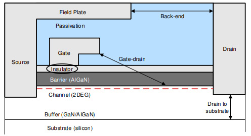
Incorrect gate control of a GaN FET will cause a breakdown of the insulative layer, barrier,g or other structural elements; the device will not only fail during that system condition, but it is likely also permanently damaged. This level of sensitivity necessitates a review of different types of Gallium Nitride devices and their broad needs. HEMTs also do not have the traditional doped FET structure that forms p-n junctions, which then cause body diodes. This means that there are no internal diodes that can break down or cause unwanted behavior during operation such as reverse recovery.
Gate driver and bias supply considerations
Enhancement-mode (e-mode) GaN FETs look very similar to the e-mode silicon FETs with which you may already be familiar. A positive voltage of 1.5 V to 1.8 V will begin turning on the FET, with most operating conditions specified for 6-V gate threshold operation. However, most e-mode GaN devices have a maximum gate threshold of 7 V, which when violated will likely result in permanent damage.
If traditional silicon gate drivers do not offer proper voltage regulation or cannot handle the high common-mode transient immunity in a GaN-based design, many designers choose a gate driver such as the Texas Instruments (TI) LMG1210, which is designed specifically for use with a GaN FET. The LMG1210 offers a gate drive voltage of 5 V, regardless of supply voltage. Traditional gate drivers need very tight regulation of the gate driver’s bias supply so that they do not overstress the GaN FET. A cascode GaN FET, shown in Figure 3, is a compromise for ease of use compared with e-mode GaN FETs.
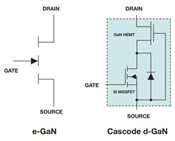
The GaN FET is a depletion-mode (d-mode) device, which means that it is normally on and requires a negative gate threshold to turn the device off. This is extremely problematic for a power switch, so most manufacturers add a 30-V silicon FET in series with the GaN FET for sale as one package. The gate of the GaN FET connects to the source of the silicon FET and applies the turn-on and turn-off gate pulses to the gate of the silicon FET.
Having a traditional isolated gate driver such as TI’s UCC5350 drive the silicon FET eliminates many gate driver and bias supply concerns. The biggest downsides of cascode GaN FETs are the higher output capacitance of the FET and susceptibility to reverse recovery, given the presence of a body diode. The output capacitance of the silicon FET adds on to that of the GaN FET, resulting in a 20% increase, which means >20% increased switching losses compared with other Gallium Nitride solutions. And during reverse conduction, the body diode of the silicon FET conducts current and undergoes reverse recovery when the voltage polarity flips.
Cascode GaN FETs operate at slew rates of 70 V/ns (compared with 150 V/ns for other Gallium Nitride solutions) to guard against avalanche breakdown of the silicon FET, increasing switching overlap losses. Although cascode GaN FETs are simpler to design with, they limit the achievable performance.
Integration offers an easier solution
The integration of a gate driver with built-in bias supply regulation and a d-mode GaN FET solves many of the design challenges of e-mode and cascode GaN FETs. For example, TI’s LMG3422R030, a 600-V 30-mΩ Gallium Nitride device, has an integrated gate driver and power management features that enable higher power density and efficiency while reducing the risks and engineering effort required. Because the GaN FET is d-mode, there is a silicon FET integrated in series with the GaN FET. But the big difference versus cascode GaN FETs is that the integrated gate driver can directly drive the gate of the GaN FET, while the silicon FET performs the role of a normally off enabled switch at power-up. This approach, known as direct drive, eliminates the most pressing issues of cascode GaN FETs, such as higher output capacitance, reverse-recovery susceptibility, and avalanche breakdown of the silicon FET in series. The gate driver integrated in the LMG3422R030 enables very low switching overlap losses, enabling this GaN FET to operate at a switching frequency as high as 2.2 MHz and eliminating the risk of pairing the GaN FET with the wrong gate driver. Figure 4 shows an example of a half-bridge configuration using integrated LMG3422R030 GaN FETs.
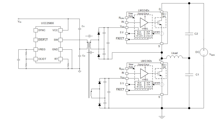
The integrated driver shrinks solution size, enabling a power-dense system. Integrating a buck-boost converter also means that the LMG3422R030 can operate with a 9-V to 18-V unregulated power supply, which significantly reduces bias supply requirements. To enable a compact and lower-cost system solution, you could combine the LMG3422R030 with an ultra-low-electromagnetic-interference transformer driver such as TI’s UCC25800, which has open-loop inductor-inductor-capacitor control with multiple secondary-side windings. Alternatively, a highly integrated, compact bias power supply such as TI’s UCC14240 DC/DC module can supply the device locally, resulting in a low-profile design with a small printed-circuit–board footprint.
Conclusion
With the right gate driver and bias supply, Gallium Nitride devices can help you achieve system-level benefits such as a switching speed of 150 V/ns, reduced switching losses, and a smaller magnetics size for high-power systems across industrial and automotive applications. Integrated Gallium Nitride solutions simplify many of your device-level challenges so that you can focus on the wider system.