SiC MOSFETs come with remarkable properties and a unipolar conduction mechanism, which leads to a reduction in their size and improved switching performance.
Although silicon is the most widely used semiconductor in electronics, recent studies show that it has some limitations, particularly in high-power applications. The bandgap is a relevant factor for semiconductor-based circuits, as a high bandgap offers advantages in terms of operation at high temperatures, voltages, and frequencies. While silicon has a bandgap of 1.12 eV, silicon carbide has a 3× greater bandgap value of 3.2 eV, leading to better performance and efficiency with higher switching frequencies, as well as a smaller overall footprint.
SiC MOSFETs come with remarkable properties and a unipolar conduction mechanism, which leads to a reduction in their size and improved switching performance. In addition, the size of SIC MOSFETs can be smaller than Si counterparts, as theorized in Huang’s figures of merit1 when having the same current and voltage ratings. Due to the smaller size, the overall parasitic capacitance is less, which enables SiC MOSFETs to achieve high switching speed and low on-state resistance. Hence, SiC-based converters have great potential for use in hybrid/electric vehicles, solar inverters, and uninterruptible power supplies.
Previous research indicates that the significant reduction in SiC chip size is considered only for the active region. The termination region that encloses the active region and helps in successfully achieving the near-ideal avalanche breakdown cannot be scaled due to the fringe electric field placed at the boundary of the active region. A team of researchers carried out work to analyze the parasitic capacitance introduced from the termination region and how it influences the switching loss for SiC MOSFETs.2 This research was supported in part by the National Natural Science Foundation of China and in part by the State Key Laboratory of Wide-Bandgap Semiconductor Power Electronic Devices. [Original article]
Analyzing SiC MOSFETs in the termination region
In the paper titled “Impact of Termination Region on Switching Loss for SiC MOSFET,” the researchers analyze the influence of the termination region on parasitic capacitances. To put it simply, parasitic capacitance is an unavoidable but undesired capacitance that exists between the parts of an electronic component or circuit because of their proximity to each other.

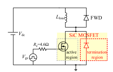
The input capacitance, output capacitance, and reverse-transfer capacitance are all dependent on the capacitances between all three terminals of the SiC MOSFET. As there is a physical overlap between the gate bus and source electrodes, the oxide layer beneath the gate is comparatively thicker than the gate oxide layer. With no overlap between gate and drain electrodes as well as gate and source terminals, they contribute very little to the overall capacitance. Therefore, the drain-to-source terminal capacitance consists of equivalent capacitances from the active and termination region.
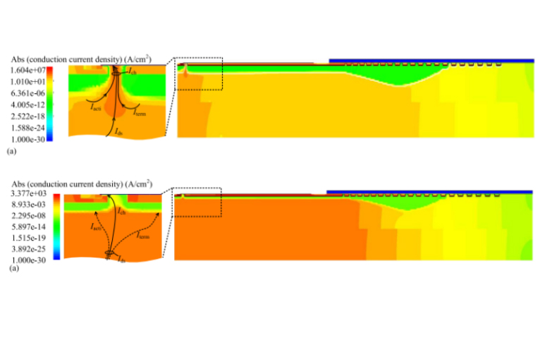
The team used TCAD Sentaurus to demonstrate the operating principles of the parasitic capacitances during turn-on and turn-off events of the SiC MOSFET. TCAD Sentaurus is an advanced multidimensional simulator that is capable of simulating electrical, thermal, and optical characteristics of silicon-based devices and is used to develop and optimize semiconductor process technologies. Overlapping of voltage (Vds) across the device and current (Ids) flowing through the device results in switching losses. To illustrate the switching process inside the SiC MOSFET, channel current (Ich) is introduced through the gate channel.
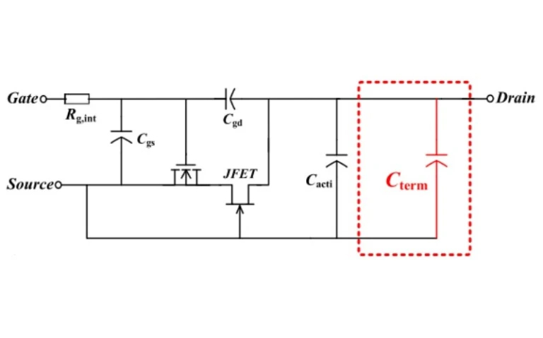
During the Miller interval of the turn-on process, gate-to-drain capacitance (Cgd) and active region capacitance (Cacti) are discharged due to the resistive flow of discharging current (Iterm) from the capacitance introduced in the termination region (Cterm) through the gate channel located in the active region. The dissipative current flowing through the gate channel or the channel current (Ich) in this interval is a combination of current flowing in the termination region (Iterm) along with the discharging current of the active region capacitance (Iacti) and the drain-to-source current (Ids).
While for the Miller interval of turn-off process, instead of flowing through the gate channel, a portion of drain-to-source current (Ids) starts charging the capacitance introduced in the active and the termination region (Cacti and Cterm), as shown in the figure below. Here, the dissipative channel current (Ich) excludes the currents of Cterm and Cacti (i.e., Ich = Ids – Iacti – Iterm).
Modeling of switching loss for SiC MOSFETs
During the physical analysis of the termination region, the channel current (Ich) flowing through the gate channel of the SiC MOSFET is the essential current demonstrating switching loss but not measurable drain-to-source current (Ids). Hence, the turn-on and turn-off loss expressions considering the termination region are given as:
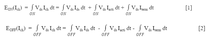
After combining the above equations for turn-off and turn-on loss expressions, the following equations are defined:
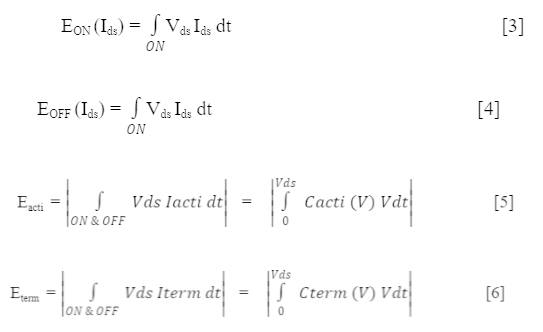
Equations 3 and 4 represent the switching loss contribution from the measurable Ids during the turn-on and turn-off Miller processes. Equations 5 and 6 depict the charging and discharging of Cacti and Cterm. For a given device, the energy stored in parasitic capacitances from the active region and the termination region is fixed with the same blocking voltage but independent of Ids.
Results
As shown in Figure 4, a double-pulsed test with a SiC MOSFET split in the active region and termination region is built to check the composition of switching loss. The rating currents of the SiC MOSFET are 1, 3, and 6 A, which is defined when Vds = 3 V and Vgs = 20 V. Using a TCAD Sentaurus simulation, the calculated switching loss breakdowns of 1-, 3-, and 6-A SiC MOSFETs under 800, 1,000, and 1,200 V are shown in the below figure.
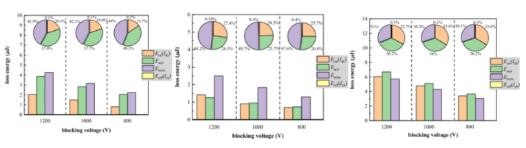
The switching loss is broken down into EON (Ids), Eacti, Eterm, and EOFF (Ich). The values of EON (Ids), Eacti, and Eterm are comparative, while EOFF (Ich) becomes very low under various blocking voltages and current ratings. With the increase in the area for the active region for higher current ratings, Eacti increases the proportion of total switching loss. If a relatively weaker gate driver is used, EON (Ids) and EOFF (Ich) will be greater. On the other hand, Eacti and Eterm are fixed for a specific MOSFET. For EOFF of SiC MOSFET, little current flows through the gate channel generating little joule heating but almost all the current charges the Cacti and Cterm as displacement current. This results in a lower value of EOFF (Ich). It can be expressed as follows:
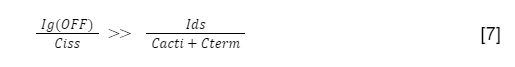
Where Ig(OFF) is the discharge current of the gate loop during the turn-off process, it indicates that the turn-off duration is much faster than the Cacti and Cterm .
Conclusion
The physical insights into the termination region of the SiC MOSFET are simulated using TCAD Sentaurus and the switching loss model considering the impact of termination regions. It was verified that the impact of the termination region on switching loss cannot be overlooked, particularly for low-current–rated SiC MOSFETs. One of the significant parts of turn-on loss is Eterm and Eacti,which is an intrinsic loss with or even higher than the commonly used electric measurement estimation.
EON should include Eterm and Eacti, whereas EOFF should exclude Eterm and Eacti compared with conventional switching loss estimation. The consideration of Cterm further aggravates the underestimation and overestimation of EON and EOFF, respectively. The inaccurate loss estimation could influence SiC MOSFET choice and applied circuit design for specific applications.
References
1A. Q. Huang. “New unipolar switching power device figures of merit.” IEEE Electron. Device Lett., Vol. 25, No. 5, pp. 298–301, May 2004.
2Li et al. “Impact of Termination Region on Switching Loss for SiC MOSFET.” IEEE Transactions on Electron Devices, Vol. 66, No. 2, pp. 1026–1031, February 2019, doi: 10.1109/TED.2018.2888995.