This article analyzes the successful co-integration of high-performance Schottky barrier diodes and D-mode HEMTs on a p-GaN HEMT–based 200-V GaN-on-SOI smart power IC platform. The addition of these components enables the design of chips with extended functionality and increased performance that takes monolithically integrated GaN power ICs one step further. This achievement paves the way toward smaller and more efficient DC/DC converters and PoL converters.
GaN: The answer to Silicon for power electronics
For decades, silicon-based power transistors such as MOSFETs formed the backbone of power-conversion systems that convert alternating current (AC) into direct current (DC) and vice versa, or DC from low voltage to high voltage and vice versa. In the quest for alternatives that can drive up the switching speed, gallium nitride quickly came forward as one of the leading candidate materials. The GaN/AlGaN materials system exhibits a higher electron mobility and higher critical electric field for breakdown. Combined with the high-electron–mobility transistor (HEMT) architecture, it results in devices and ICs that feature higher breakdown strength, faster switching speed, lower conductance losses, and a smaller footprint than comparable silicon solutions.

Today, most GaN power systems are formed from multiple chips. GaN-based devices are assembled as discrete components before they are united on a printed-circuit board. The downside of that approach is the presence of parasitic inductances that affect the performance of the devices.
Take a driver, for example. Discrete transistors with drivers on a separate chip suffer a lot from parasitic inductances between the output stages of the driver and the input of the transistor and in the switching node of half-bridges. GaN HEMTs have very high switching speed, which leads to ringing — an unwanted oscillation of the signal — when the parasitic inductance is not suppressed. The best way to reduce the parasitics and exploit the superior switching speed of GaN is to integrate both driver and HEMT on the same chip.
At the same time, it reduces the dead-time control between two transistors in a half-bridge, wherein one transistor has to switch off just as the other one switches on. During the time in between, there is a short-circuit between the power source and the ground, or dead time. Integrating all components on-chip will address the ringing, reduce dead time, and ultimately improve the power efficiency of your converter.
Co-integration of D-Mode HEMTs
Imec has already made tremendous progress monolithically integrating building blocks on a silicon-on-insulator (SOI) substrate such as drivers, half-bridges, and control/protection circuits. Now, researchers have succeeded in adding two sought-after components to the portfolio: depletion-mode (D-mode) HEMTs and Schottky diodes.
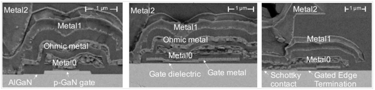
(a) E-mode p-GaN HEMT; (b) D-mode MIS HEMT; (c) Schottky barrier diode. All devices include metal field plates based
on front-end and interconnect metal layers and separated by dielectric layers.
One of the main remaining hurdles to boost the full performance of GaN power ICs is finding a suitable solution for the lack of p-channel devices in GaN with acceptable performance. CMOS technology uses complementary and more symmetrical pairs of p- and n-type FETs, based on the mobilities of holes and electrons for both types of FETs. However, in GaN, the mobility of holes is about 60× worse than that of electrons; in silicon, this is a factor of only 2. That means a p-channel device, in which holes are the principal carriers, would be 60× larger than the n-channel counterpart and highly inefficient. A widespread alternative is replacing the P-MOS with a resistor . Resistor-transistor logic (RTL) has been employed for GaN ICs but shows tradeoffs between switching time and power consumption.
Imec has improved the performance of GaN ICs by co-integrating D-mode HEMTS on its functional enhancement-mode (E-mode) HEMT platform on SOI. Enhancement and depletion mode refer to an on (D-mode) or off (E-mode) state at zero source voltage, resulting in a current flow (or not) in the transistor. Imec expects that taking the step from RTL to direct-coupled FET logic will improve speed and reduce the power dissipation of the circuits.
Schottky diodes with low leak currents
The integration of a Schottky barrier diode further boosted the power efficiency of GaN power ICs. In comparison with Si diodes, they can withstand higher voltages for the same on-state resistance or lower on-state resistance for the same breakdown voltage.
The challenge in making Schottky barrier diodes is to obtain low turn-on voltage and, at the same time, a low leakage level. Unfortunately, when you aim for lower turn-on voltages, you will end up with a small barrier to hold off the leakage current, and Schottky diodes are notorious for having high leak currents. Imec’s proprietary gate-edge–terminated Schottky-barrier–diode architecture (GET-SBD) results in a low turn-on voltage of about 0.8 V while at the same time reducing the leakage current several orders of magnitude in comparison with conventional GaN Schottky barrier diodes.
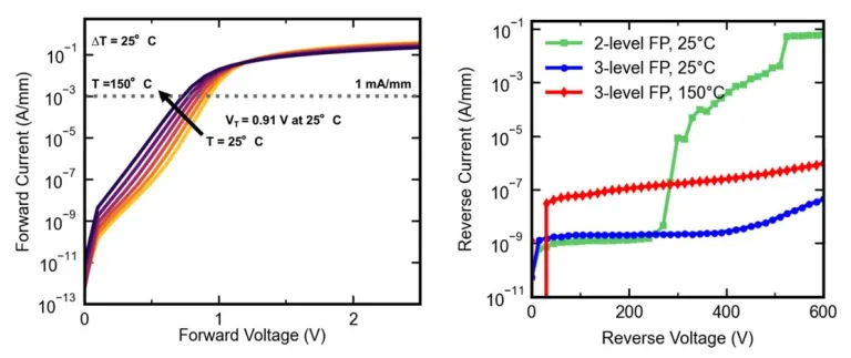
(right) low reverse leak currents (2 nA/mm for 25˚C) for two different anode field plate configurations evaluated at
25˚C and 150˚C.
Fast switches and high voltages
GaN is the go-to material for high-power applications because the critical voltage that induces breakdown of the transistor (breakdown voltage) lies 10× higher than in silicon. But GaN still has an edge over silicon in low-power applications because of its superior switching speed.
The GaN-based ICs that imec creates open the way toward smaller and more efficient DC/DC converters and point-of-load (PoL) converters. A smartphone, tablet, or laptop, for example, contains chips that work on different voltages, requiring AC/DC converters for charging the battery and PoL converters inside the devices for generating the different voltages. These components not only consist of a switch but also transformers, capacitors, and inductors. The faster the transistor can switch, the smaller these components become, ultimately resulting in a more compact and low-cost system for the same power.
Fast battery chargers form the largest market for GaN today, followed by power supplies for servers, the automotive industry, and renewable energy. It is expected that the power supplies using GaN are more reliable at the system level. They are smaller in form factor and weight, reducing the bill of materials and, hence, the cost.
Vertical devices under research
Imec will focus on improving the performance of the existing platform and perform further reliability tests. The company currently offers a 200-V and 650-V platform for prototyping, soon to be followed by 100 V. For GaN ICs with integrated components, a 1,200-V high-power platform may not yield significant improvements. The higher the voltage, the slower the components become. Therefore, it may not be necessary to integrate the driver on-chip; simulations will confirm this.
Imec is also looking into alternatives for discrete 1,200-V devices, enabling GaN technology for the highest-voltage power applications, such as electric cars. Transistors with a lateral topology are the dominant GaN device architecture today. These devices have their three terminals (source, gate, and drain) at the surface in the same plane, so the electrical field is lateral, spanning the GaN buffer layers and partly the back end (metallization, oxide). In a vertical device, the source and gate are at the surface, while the drain is at the bottom of the epi stack. The electrical field in that case flows through the whole stack. It is the source-drain separation that determines the breakdown voltage of the device, and a larger separation safeguards the channel from breakdown. However, larger distances between a laterally placed source and drain result in larger devices. Because the chips for 1,200-V devices would become too large, lateral architectures are usually advised up to 650 V maximum. For a vertical device, on the contrary, going to higher voltages boils down to creating a thicker epi stack because source and drain are located on different ends of the stack. The chip’s surface area doesn’t increase.