A team at the Ohio State University has been studying various aspects of the SiC power MOSFET reliability, including threshold voltage instability and gate oxide reliability.
The Ohio State University (OSU) has been at the forefront of reliability studies on SiC power devices. A team led by Prof. Anant Agarwal has been studying various aspects of the SiC power MOSFET reliability, including threshold voltage (Vt) instability, gate oxide reliability, body diode degradation, and Short Circuit Withstand Time (SCWT) [1-8]. In this article we will focus on the Vt instability and gate oxide reliability work at OSU, and present some of the challenges.
One of the goals for a 100kW 3-phase inverter for use in future Electric Vehicle (EV’s) chargers is a 450A to 550A rated switch for the 400V rated battery. Summaries of the largest SiC dies available today at a 650V voltage rating are listed below in Table 1.

As can be seen, several devices would have to be placed in parallel for the 3-phase power module application. This can present challenges in matching device parameters within the module. The variation and drift of the threshold voltage in the SiC MOSFET is a major concern.
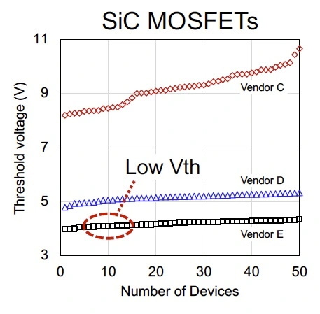
All plots below are from studies done at OSU to understand the Vt instability and gate oxide reliability in SiC MOSFETs. Figure 1 shows the Vt data at 25 for devices from three vendors that were characterized at OSU. As can be seen, some vendors have a relatively well-behaved Vt with a variation < 0.5 V, while others shown variations >3 V.
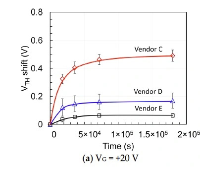
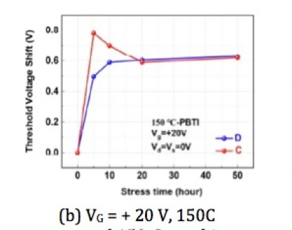
Furthermore, a bias on the gate causes the Vt to shift in the same direction as the bias voltage on the gate through tunneling of electrons from inversion layer to trap states near the SiC/oxide interface. Figures 2(a) and 2(b) show this effect at room temperature and at 150° for the same devices as above.
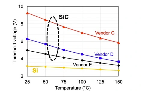
In a switching application, the junction temperature of a SiC power MOSFET can exceed 100°. The Vt of the device naturally shifts negative at higher temperatures as electrons in interface re-emit back to the conduction band, hence decreasing the negative charge within the oxide. Figure 3 shows the change in Vt vs. temperature for SiC power MOSFETs and shows a comparative curve of Si power MOSFETs. As can be seen, the device with the lowest interface states (Vendor E) and smallest Vt shift with a gate bias stress, also has a lower temperature coefficient of Vt. However, vendor E still shows a higher slope than the Si reference devices. In a parallel device operation, the positive temperature coefficient of Rds,on helps compensate the drive from a hotter device, but a variable Vt temperature coefficient among the devices makes the module unstable.
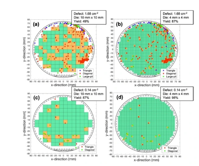
The gate oxide is the weakest link in a SiC power MOSFET. From an intrinsic (dielectric material) reliability standpoint, Si and SiC power MOSFETs with 40 nm to 80 nm oxide thickness have been shown to have similar lifetimes from Time Dependent Dielectric Breakdown (TDDB) measurements [9]. The author in this study concludes that to guarantee a low failure probability with a 20-year lifetime under typical usage conditions (Vgs = 15-20 V at 150°), a gate oxide thickness of 40 nm or higher would be sufficient. This however does not include extrinsic defects that can play a critical role for larger device sizes. Extrinsic defects can include distortions at the interface that cause localized oxide thinning [9]. Figure 4 shows the defect maps supplied by epi vendors with low (0.14/cm2) and medium (1.68/cm2) defect densities (DD) [5]. Small (4mmx 4mm) and medium (10mmx10mm) sized dies are superimposed on these maps. As shown in Figure 4, the yield on the larger die suffers considerably as DD increases.
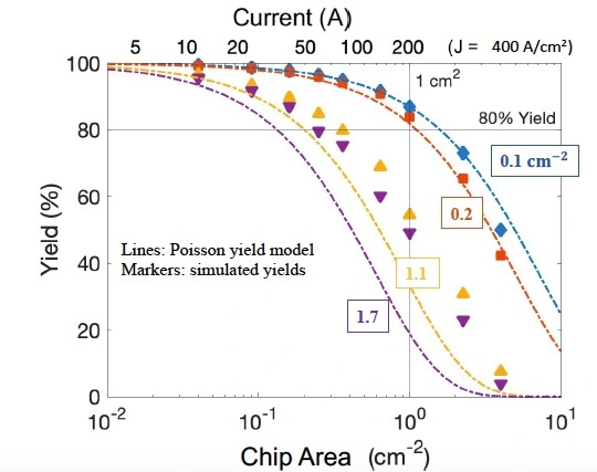
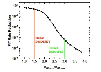
Figure 5 shows the yield predictions using the Poisson yield model for different DD and die sizes. To achieve >80% yield on a 1cm2 die for larger current applications, DD needs to be below 0.2/cm2. Screening of extrinsic defects is essential to ensure part reliability. Experiments have concluded that the electric field used during such the screening needs to be <= 9 MV/cm in order to avoid hole trapping mechanisms that can accelerate the degradation of device lifetime [3, 4]. For a typical 40nm gate oxide used in planar SiC MOSFETs, this would mean a screening voltage (Vscr) to usage Vgs (Vguse) ratio of around 1.5. Figure 6, reproduced from [9], shows a FIT rate (failure per billion device hours) reduction vs. Vscr/Vguse ratio. The ratio of 1.5 would be insufficient to screen the defects. To this end, studies have been concluded showing that trench SiC power MOSFETs offer an advantage in their ability to use a thicker gate oxide compared to the planar version, taking advantage of higher channel mobility on the vertical plane as well as a smaller device pitch. This allows the use of a thicker gate oxide and hence a higher Vscr/Vguse ratio [9]. Figure 6 shows a much better screening improvement in FIT rate using a Vscr/Vguse ratio of 3 in the trench SiC power MOSFET.
Further studies are needed to optimize the screening for a given gate oxide. As the gate oxide interface charge is improved [10], a corresponding improvement also needs to be made to the fixed charges in the gate oxide to keep the Vt in the enhancement mode and more dependent on doping levels rather than oxide charges, as in Silicon. Wafer level stress tests at higher temperatures (>= 150°) can accelerate the Vt or leakage degradation from extrinsic defects in the oxide and reduce screening test times as well.